RL78/G15 CHAPTER 13 SERIAL INTERFACE IICA
R01UH0959EJ0110 Rev.1.10 Page 523 of 765
Mar 7, 2023
13.3.5 IICA control register 01 (IICCTL01)
This register is used to set the operation mode of I
2
C and detect the states of the SCLA0 and SDAA0 pins.
The IICCTL01 register can be set by a 1-bit or 8-bit memory manipulation instruction. However, the CLD0 and DAD0 bits
are read-only.
Set the IICCTL01 register, except the WUP0 bit, while operation of I
2
C is disabled (bit 7 (IICE0) of IICA control register
00 (IICCTL00) = 0).
Reset signal generation clears this register to 00H.
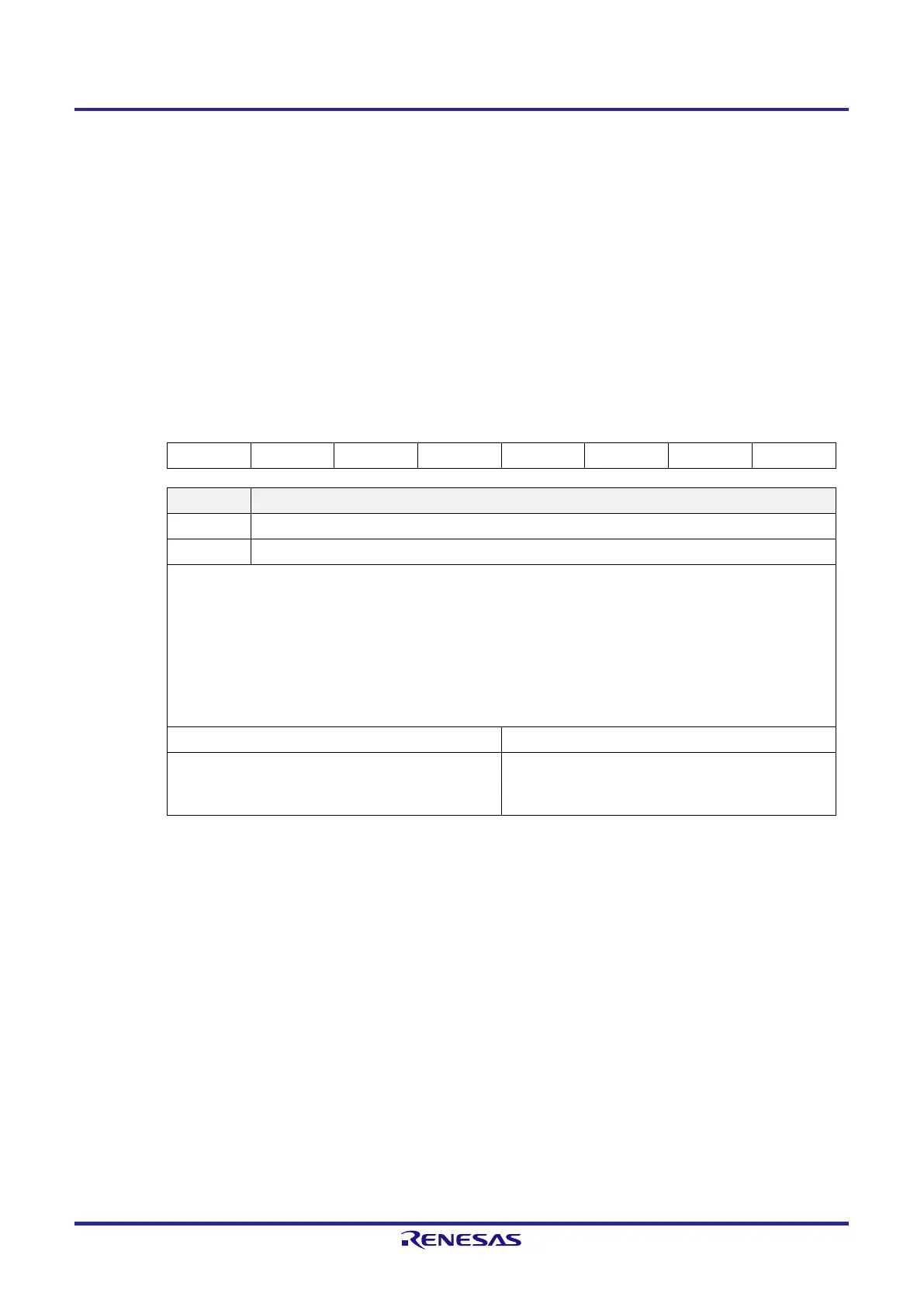
Figure 13-9. Format of IICA Control Register 01 (IICCTL01) (1/2)
Address: F0231H After reset: 00H R/W
Note 1
Symbol
□
7 6
□
5
□
4
□
3
□
2 1 0
IICCTL01 WUP0 0 CLD0 DAD0 SMC0 DFC0 0 0
WUP0 Control of address match wakeup
0 Stops operation of address match wakeup while in STOP mode.
1 Enables operation of address match wakeup while in STOP mode.
To shift to STOP mode when WUP0 = 1, execute the STOP instruction at least three cycles of f
CLK
after setting (1) the
WUP0 bit (see Figure 13-21 Flow when Setting WUP0 = 1).
Clear (0) the WUP0 bit after an address match or reception of an extension code. Clearing (0) the WUP0 bit allows
participation in subsequent communications (releasing clock stretching and writing transmit data must follow clearing (0)
the WUP0 bit).
The interrupt timing on an address match or extension code reception while WUP0 = 1 is the same as the interrupt
timing when WUP0 = 0 (a delay difference equivalent to the sampling error by the clock is generated). Furthermore,
when WUP0 = 1, a stop condition interrupt is not generated even if the SPIE0 bit is set to 1.
Condition for clearing (WUP0 = 0) Condition for setting (WUP0 = 1)
●
Cleared by instruction (after address match or
extension code reception)
●
Set by instruction (when MSTS0, EXC0, and COI0 = 0
and STD0 = 0 (non-participation in communications)
Note
2
 Loading...


