RL78/G15 CHAPTER 13 SERIAL INTERFACE IICA
R01UH0959EJ0110 Rev.1.10 Page 524 of 765
Mar 7, 2023
Figure 13-9. Format of IICA Control Register 01 (IICCTL01) (2/2)
CLD0 SCLA0 pin level detection (valid only when IICE0 = 1)
0 The SCLA0 pin was detected to be at the low level.
1 The SCLA0 pin was detected to be at the high level.
Condition for clearing (CLD0 = 0) Condition for setting (CLD0 = 1)
●
When the SCLA0 pin is at the low level
●
When IICE0 = 0 (operation stop)
●
Reset
●
When the SCLA0 pin is at the high level
DAD0 SDAA0 pin level detection (valid only when IICE0 = 1)
0 The SDAA0 pin was detected be at the low level.
1 The SDAA0 pin was detected to be at high level.
Condition for clearing (DAD0 = 0) Condition for setting (DAD0 = 1)
●
When the SDAA0 pin is at the low level
●
When IICE0 = 0 (operation stop)
●
Reset
●
When the SDAA0 pin is at the high level
SMC0 Operation mode switching
0 Operates in standard mode (maximum transfer rate: 100 kbps).
1 Operates in fast mode (maximum transfer rate: 400 kbps)
DFC0 Digital filter operation control
0 Digital filter off
1 Digital filter on
Use the digital filter only in fast mode.
The digital filter is used for noise elimination.
Set (1) or clearing (0) the DFC0 bit does not vary the transfer clock.
Note 1. Bits 5 and 4 are read-only.
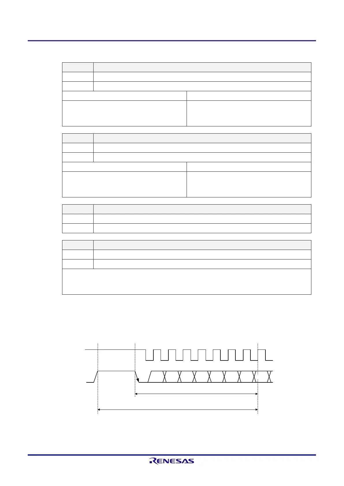
Note 2. The WUP0 bit must be set after checking the state of IICA status register 0 (IICS0) during the period shown
below.
SCLA0
<1> <2>
SDAA0
A6 A5 A4 A3 A2 A1 A0
The maximum time from reading IICS0 to setting WUP is a period from
<1> to <2>.
Check the operation state with IICS0 and set WUP0 during this period.
__
R/W
 Loading...


