RL78/G15 CHAPTER 10 A/D CONVERTER
R01UH0959EJ0110 Rev.1.10 Page 322 of 765
Mar 7, 2023
10.3.2 A/D converter mode register 0 (ADM0)
This register sets the time for converting analog input to digital data, and starts and stops conversion operation.
The ADM0 register can be set by a 1-bit or 8-bit memory manipulation instruction.
Reset signal generation clears this register to 00H.
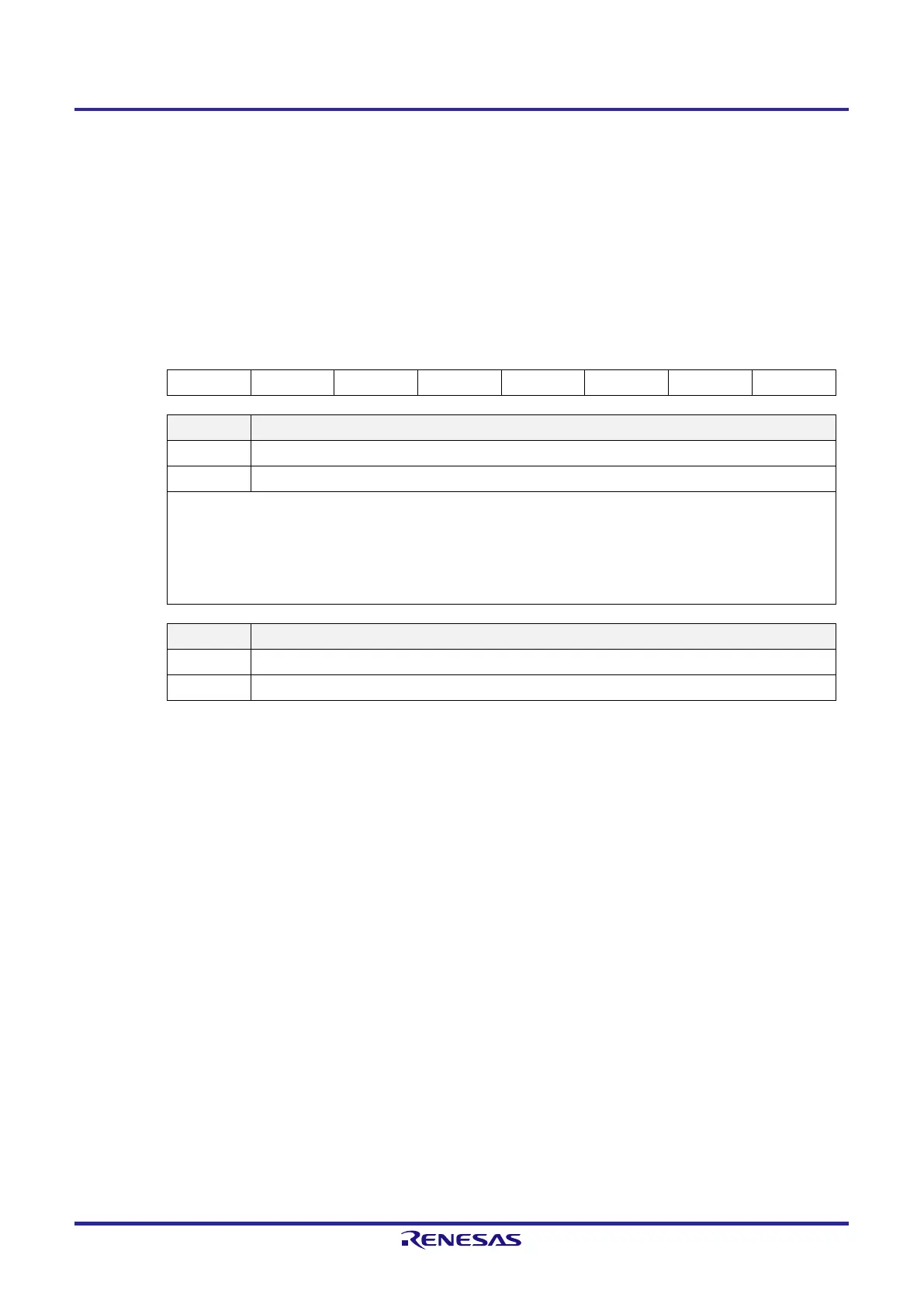
Figure 10-3. Format of A/D Converter Mode Register 0 (ADM0)
Address: FFF30H After reset: 00H R/W
Symbol
□
7 6 5 4 3 2 1
□
0
ADM0 ADCS 0 0 FR1
Note 1
FR0
Note 1
0 LV0
Note 1
ADCE
ADCS A/D conversion operation control
0 Stops conversion operation (conversion stopped/standby state)
1 Enables conversion operation (conversion operation state)
<Clear conditions>
●
0 is written to ADCS.
●
The bit is automatically cleared to 0 when A/D conversion ends.
<Set condition>
●
1 is written to ADCS when ADCE = 1.
ADCE A/D voltage comparator operation control
Note 2
0 Stops A/D voltage comparator operation
1 Enables A/D voltage comparator operation
Note 1. For details of the FR1, FR0, and LV0 bits and A/D conversion, see Table 10-2 10-Bit Resolution A/D
Conversion Time Selection or Table 10-3 8-Bit Resolution A/D Conversion Time Selection.
Note 2. The operation of the A/D voltage comparator is controlled by the ADCS and ADCE bits, and it takes 0.125 μs
from the start of operation for the operation to stabilize. Therefore, when the ADCS bit is set to 1 after 0.125
μs or more have elapsed from the time ADCE bit is set to 1, the conversion result at that time has priority over
the first conversion result. If the ADCS bit is set to 1 to perform A/D conversion without waiting for at least
0.125 μs, ignore data of the conversion.
Caution 1. Only rewrite the FR1, FR0, and LV0 bits while in the conversion standby state (ADCS = 0, ADCE =
1) or conversion is stopped (ADCS = 0, ADCE = 0). Rewriting the values of the FR1, FR0, and LV0
bits, and ADCS bits by an 8-bit manipulation instruction at the same time is prohibited.
Caution 2. Setting ADCS = 1 and ADCE = 0 is prohibited. When 1 is written to the ADCS bit while conversion is
stopped (ADCE = 0, ADCS = 0), the ADCS bit is not set to 1.
Caution 3. Do not change the ADCS and ADCE bits from 0 to 1 at the same time by using an 8-bit
manipulation instruction. Be sure to follow the procedure described in 10.7 A/D Converter Setup
Flowchart.
Caution 4. Be sure to clear bits 2, 5, and 6 to 0.
Caution 5. Setting the ADCS bit to 1 again during conversion (ADCS = 1) is prohibited. When re-conversion by
the same channel is required, stop the conversion operation once (ADCS = 0), and then restart A/D
conversion (ADCS = 1).
 Loading...


