RL78/G15 CHAPTER 17 SELECTABLE POWER-ON-RESET CIRCUIT
R01UH0959EJ0110 Rev.1.10 Page 646 of 765
Mar 7, 2023
17.3 Operation of Selectable Power-on-reset Circuit
Specify the voltage detection level by using the option byte 000C1H.
The internal reset signal is generated at power on.
The internal reset status is retained until the supply voltage (V
DD
) exceeds the voltage detection level (V
SPOR
). The
internal reset is cleared when the supply voltage (V
DD
) exceeds the voltage detection level (V
SPOR
).
The internal reset is generated when the supply voltage (V
DD
) drops lower than the voltage detection level (V
SPDR
).
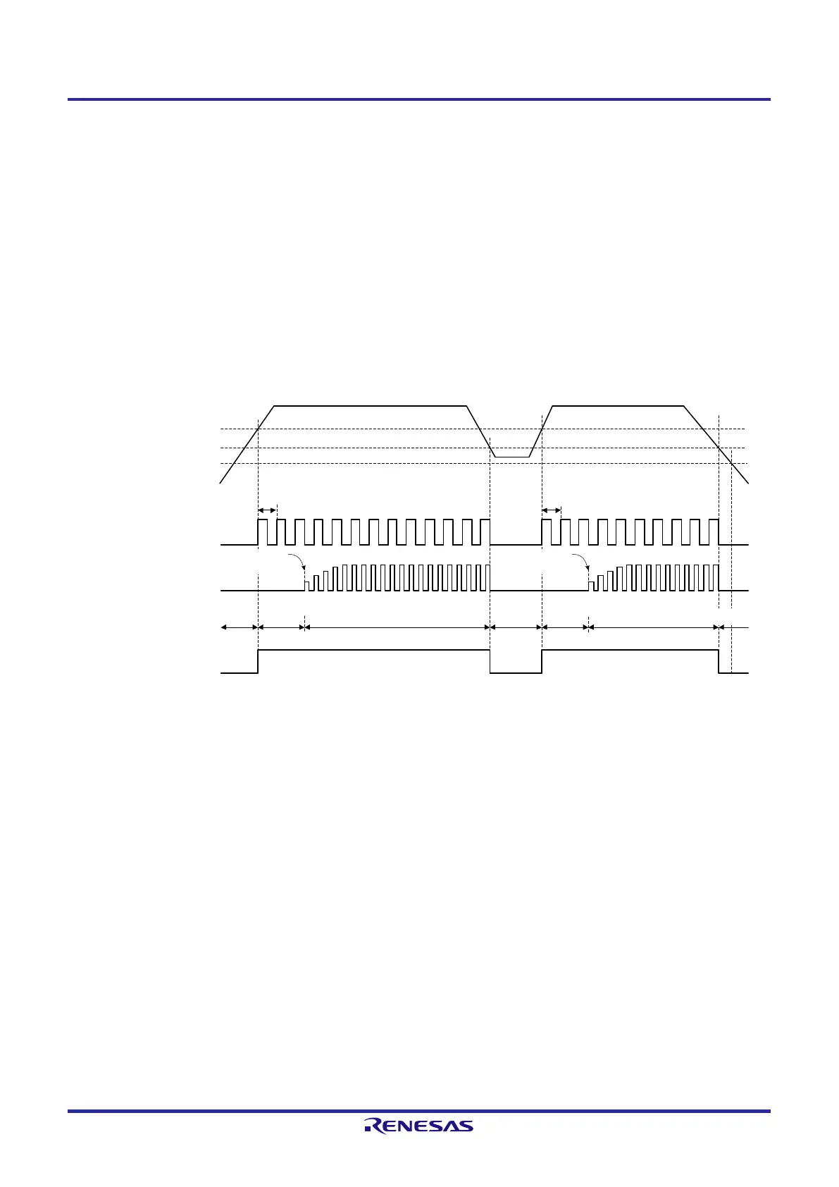
Figure 17-2 shows the timing of generation of the internal reset signal by the selectable power-on-reset circuit.
Figure 17-2. Timing of Internal Reset Signal Generation
V
DDDR
V
SPDR
V
SPOR
Supply voltage (V
DD
)
High-speed on-chip
oscillator clock (f
H
)
High-speed system clock (f
MX
)
(when X1 oscillation is selected)
(16-pin and 20-pin products only)
CPU clock
SPOR reset
processing time
3.01 ms
(MAX.)
Operation
stops
________________
Internal reset signal
Normal operation
(high-speed on-chip oscillator clock)
Note 2
Reset period
(oscillation stop)
SPOR reset
processing time
3.01 ms
(MAX.)
Starting oscillation
is specified by
software
Starting oscillation
is specified by
software
Wait for oscillation accuracy stabilization
Note 1
Wait for oscillation accuracy stabilization
Note 1
Operation
stops
Normal operation
(high-speed on-chip oscillator clock)
Note 2
Note 1. The internal reset processing time includes the oscillation accuracy stabilization time of the high-speed on-
chip oscillator clock.
Note 2. The high-speed on-chip oscillator clock and a high-speed system clock can be selected as the CPU clock
(16-pin and 20-pin products only).
To use the X1 clock, use the oscillation stabilization time counter status register (OSTC) to confirm the lapse
of the oscillation stabilization time.
Remark V
SPOR
: SPOR power supply rise detection voltage
V
SPDR
: SPOR power supply fall detection voltage
V
DDDR
: Data retention lower limit voltage
 Loading...


