RL78/G15 CHAPTER 10 A/D CONVERTER
R01UH0959EJ0110 Rev.1.10 Page 321 of 765
Mar 7, 2023
10.3.1 Peripheral enable register 0 (PER0)
The PER0 register is used to enable or disable the supply of a clock signal to various on-chip peripheral modules. Clock
supply to an on-chip peripheral module that is not to be used can be stopped to decrease power consumption and noise.
If the A/D converter is to be used, be sure to set bit 5 (ADCEN) of this register to 1.
The PER0 register can be set by a 1-bit or 8-bit memory manipulation instruction.
Reset signal generation clears this register to 00H.
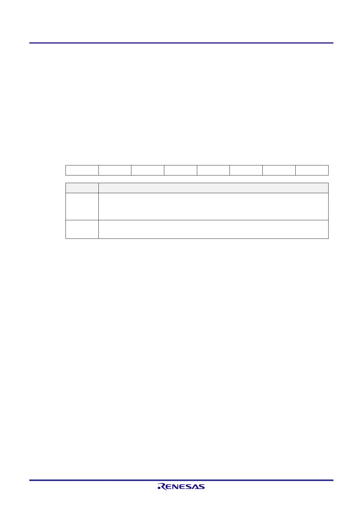
Figure 10-2. Format of Peripheral Enable Register 0 (PER0)
Address: F00F0H After reset: 00H R/W
Symbol
□
7
□
6
□
5
□
4 3
□
2 1
□
0
PER0 TMKAEN CMPEN ADCEN IICA0EN 0 SAU0EN 0 TAU0EN
ADCEN Control of A/D converter input clock supply
0 Stops supply of an input clock.
●
The SFRs used by the A/D converter cannot be written.
●
The A/D converter is in the reset state.
1 Enables supply of an input clock.
●
The SFRs used by the A/D converter can be read/written.
Caution 1. When setting the A/D converter, make sure that ADCEN = 1 before setting the following registers. If
ADCEN = 0, the values of the A/D converter control registers are cleared to their initial values and
writing to them is ignored (except for port mode registers 0 and 2 (PM0, PM2) and port mode
control registers 0 and 2 (PMC0, PMC2)).
A/D converter mode register 0 (ADM0)
A/D converter mode register 2 (ADM2)
10-bit A/D conversion result register (ADCR)
8-bit A/D conversion result register (ADCRH)
Analog input channel specification register (ADS)
A/D test register (ADTES)
Caution 2. Be sure to clear bits 1 and 3 to 0.
 Loading...


