RL78/G15 CHAPTER 8 CLOCK OUTPUT/BUZZER OUTPUT CONTROLLER
R01UH0959EJ0110 Rev.1.10 Page 306 of 765
Mar 7, 2023
CHAPTER 8 CLOCK OUTPUT/BUZZER OUTPUT
CONTROLLER
8.1 Functions of Clock Output/Buzzer Output Controller
The clock output controller is intended for clock output for supply to peripheral ICs. Buzzer output is a function to output a
square wave of buzzer frequency.
One pin can be used to output a clock or buzzer sound.
The PCLBUZ0 pin outputs a clock selected by clock output select register 0 (CKS0).
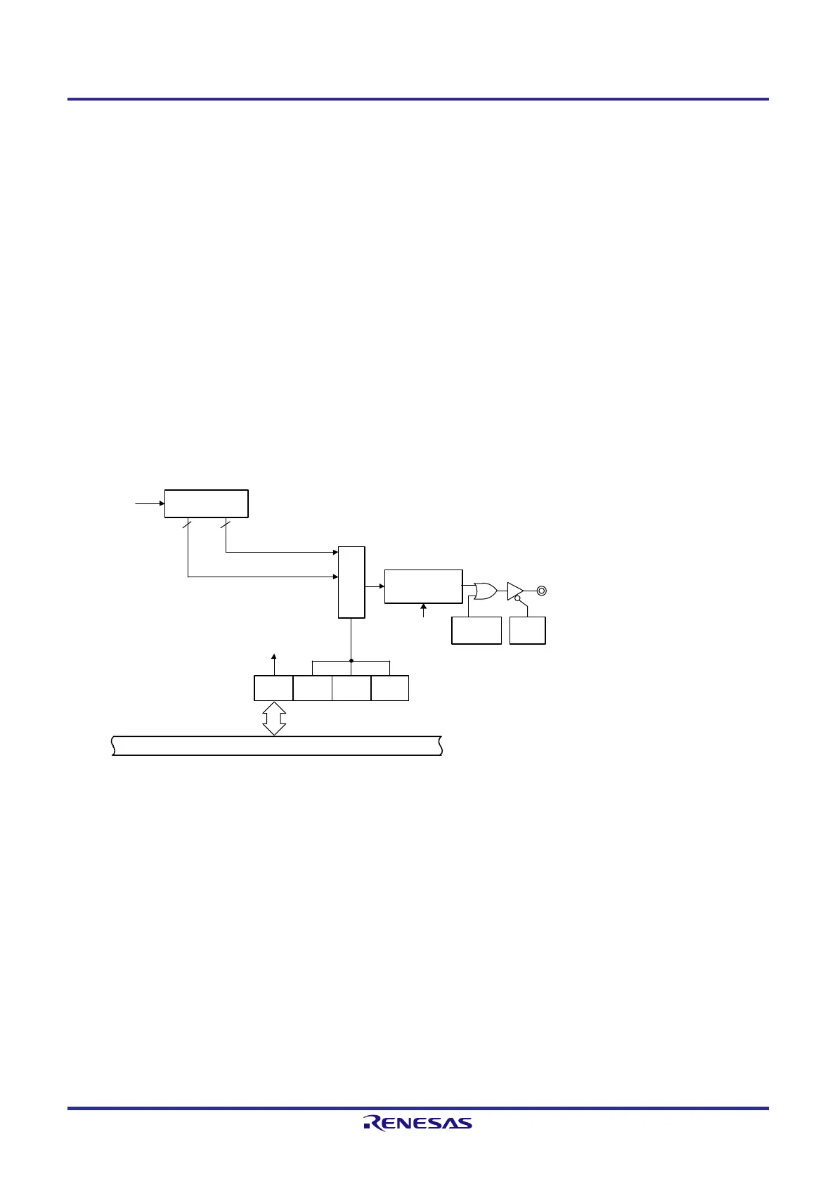
Figure 8-1 shows a block diagram of the clock output/buzzer output controller.
Figure 8-1. Block Diagram of Clock Output/Buzzer Output Controller
Prescaler
Clock/
buzzer controller
Internal bus
f
MAIN
PCLOE0
5
3
Clock output select register 0 (CKS0)
PM02
Output latch
P
02
f
MAIN
/2
11
to f
MAIN
/2
13
f
MAIN
to f
MAIN
/2
4
P02/
ANI1/VCOUT0/SCK00/SCL00/PCLBUZ0/
INTP7
/(TI
01/TO
01)/(SO01)
CCS00
PCLOE0
CCS
02
CCS01
Selector
Caution 1. For output frequencies available from the PCLBUZ0 pin, refer to 23.4 AC Characteristics and 24.4
AC Characteristics.
Remark The clock output/buzzer output pins in the above diagram are those when PIOR31 = 0 and PIOR30 = 0 in 16-
pin and 20-pin products and when PIOR30 = 0 in 10-pin products.
 Loading...


