RL78/G15 CHAPTER 4 PORT FUNCTIONS
R01UH0959EJ0110 Rev.1.10 Page 105 of 765
Mar 7, 2023
4.3.2 Port registers 0, 2, 4, 12, 13 (P0, P2, P4, P12, P13)
These registers set the output latch value of a port.
If the data is read in the input mode, the pin level is read. If it is read in the output mode, the output latch value is
read
Note 1
.
These registers can be set by a 1-bit or 8-bit memory manipulation instruction.
Reset signal generation sets the P13 register to the undefined value, and clears the other registers to 00H.
Note 1. When a pin that is set as an analog input pin (PMCxx = 1, PMxx = 1) is read, the value read is always 0
regardless of the input signal level on the pin.
When the data bit for P125 is read while the setting for the P125/RESET
¯¯¯¯¯¯
/INTP1/(VCOUT0)/(VCOUT1)/(SI01)
pin is RESET
¯¯¯¯¯¯
input (PORTSELB = 1), the value read is always 1.
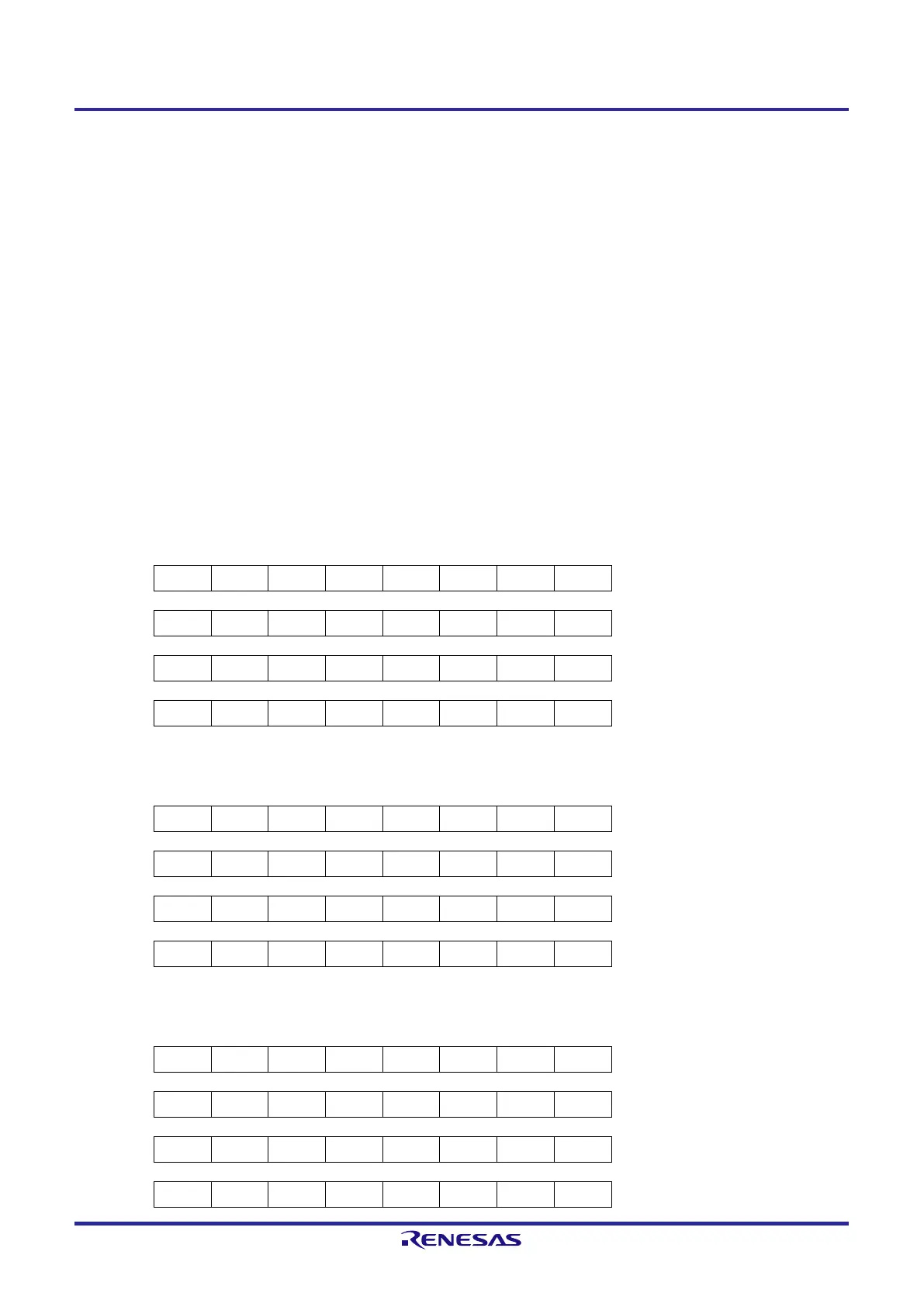
Figure 4-2. Format of Port Registers 0, 2, 4, 12, 13 (P0, P2, P4, P12, P13)
8-pin products
Symbol 7 6 5 4 3 2 1 0 Address After reset R/W
P0 0 0 0 P04 P03 0 P01 0 FFF00H 00H (output latch) R/W
P4 0 0 0 0 0 0 0 P40 FFF04H 00H (output latch) R/W
P12 0 0 P125 0 0 0 0 0 FFF0CH 00H (output latch) R/W
P13 P137 0 0 0 0 0 0 0 FFF0DH Undefined R
10-pin products
Symbol 7 6 5 4 3 2 1 0 Address After reset R/W
P0 0 0 0 P04 P03 P02 P01 P00 FFF00H 00H (output latch) R/W
P4 0 0 0 0 0 0 0 P40 FFF04H 00H (output latch) R/W
P12 0 0 P125 0 0 0 0 0 FFF0CH 00H (output latch) R/W
P13 P137 0 0 0 0 0 0 0 FFF0DH Undefined R
16-pin products
Symbol 7 6 5 4 3 2 1 0 Address After reset R/W
P0 P07 P06 P05 P04 P03 P02 P01 P00 FFF00H 00H (output latch) R/W
P4 0 0 0 0 0 0 P41 P40 FFF04H 00H (output latch) R/W
P12 0 0 P125 0 0 P122 P121 0 FFF0CH 00H (output latch) R/W
P13 P137 0 0 0 0 0 0 0 FFF0DH Undefined R
 Loading...


