RL78/G15 CHAPTER 2 PIN FUNCTIONS
R01UH0959EJ0110 Rev.1.10 Page 50 of 765
Mar 7, 2023
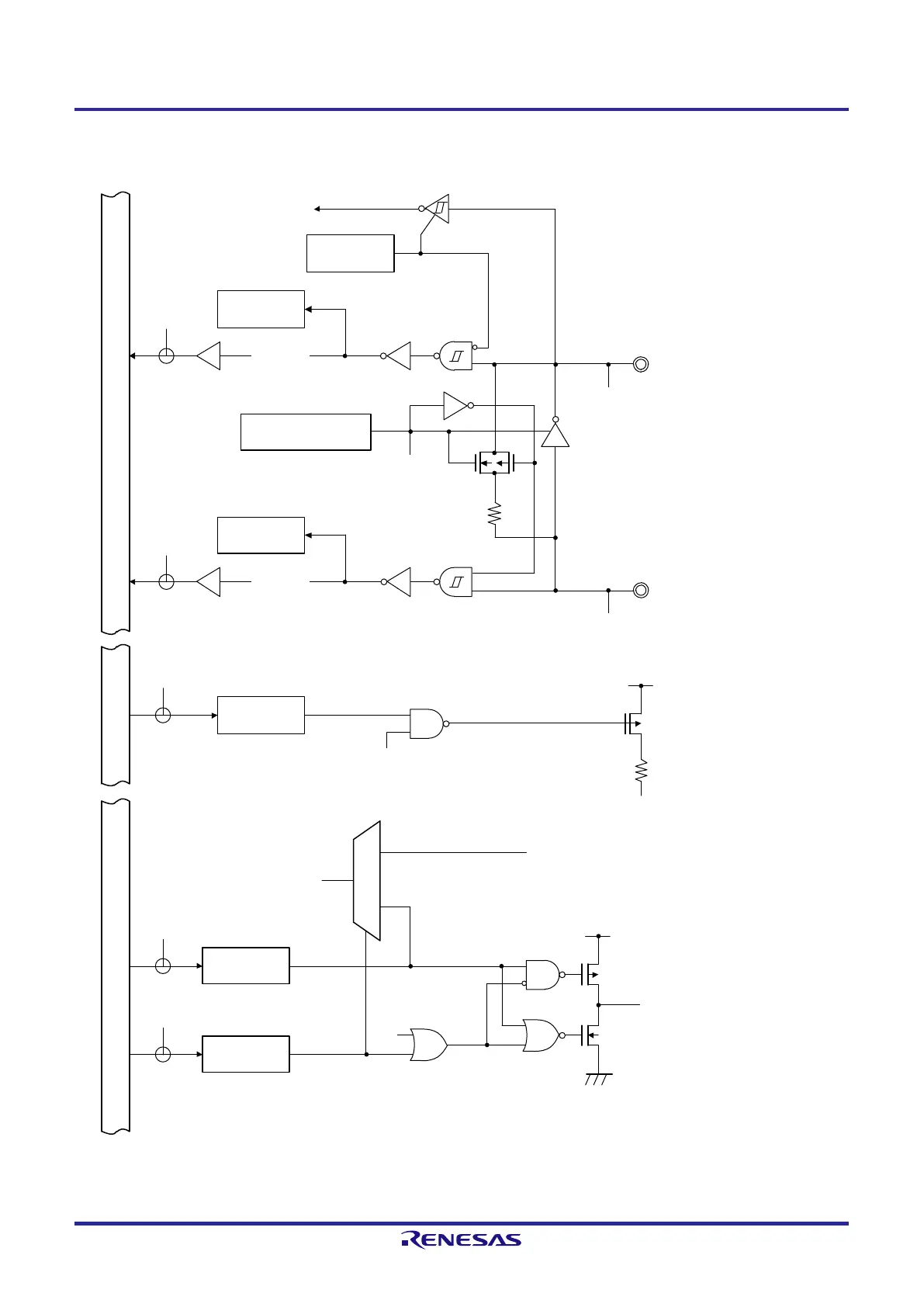
Figure 2-5. Pin Block Diagram for Pin Type 7-2-2
RD
PORT
<1>
Alternate
function
<3>
OSCSEL
P122/X2/EXCLK/Alternate function
CMC
Clock generator
EXCLK, OSCSEL
CMC
<5>
P-chN-ch
RD
PORT
<2>
Alternate
function
<4>
<6>
P121/X1/Alternate function
PU register
(PUmn)
WR
PU
V
DD
P-ch
<5>
<6>
PMmn
Output latch
(Pmn)
WR
PORT
PM register
(PMmn)
WR
PM
P-ch
N-ch
V
DD
V
SS
<5>
<6>
1
0
<3>
<4>
<1>
<2>
<7>
<7>
Internal busInternal busInternal bus
Remark 1. For alternate functions, see 2.1 Port Function.
 Loading...


