128 KByte Flash Module (S12FTMRG128K1V1)
MC9S12G Family Reference Manual Rev.1.27
1034 NXP Semiconductors
CCOBIX bits are readable and writable while remaining bits read 0 and are not writable.
29.3.2.4 Flash Reserved0 Register (FRSV0)
This Flash register is reserved for factory testing.
All bits in the FRSV0 register read 0 and are not writable.
29.3.2.5 Flash Configuration Register (FCNFG)
The FCNFG register enables the Flash command complete interrupt and forces ECC faults on Flash array
read access from the CPU.
CCIE, IGNSF, FDFD, and FSFD bits are readable and writable while remaining bits read 0 and are not
writable.
Table 29-12. FCCOBIX Field Descriptions
Field Description
2–0
CCOBIX[1:0]
Common Command Register Index— The CCOBIX bits are used to select which word of the FCCOB register
array is being read or written to. See 29.3.2.11 Flash Common Command Object Register (FCCOB),” for more
details.
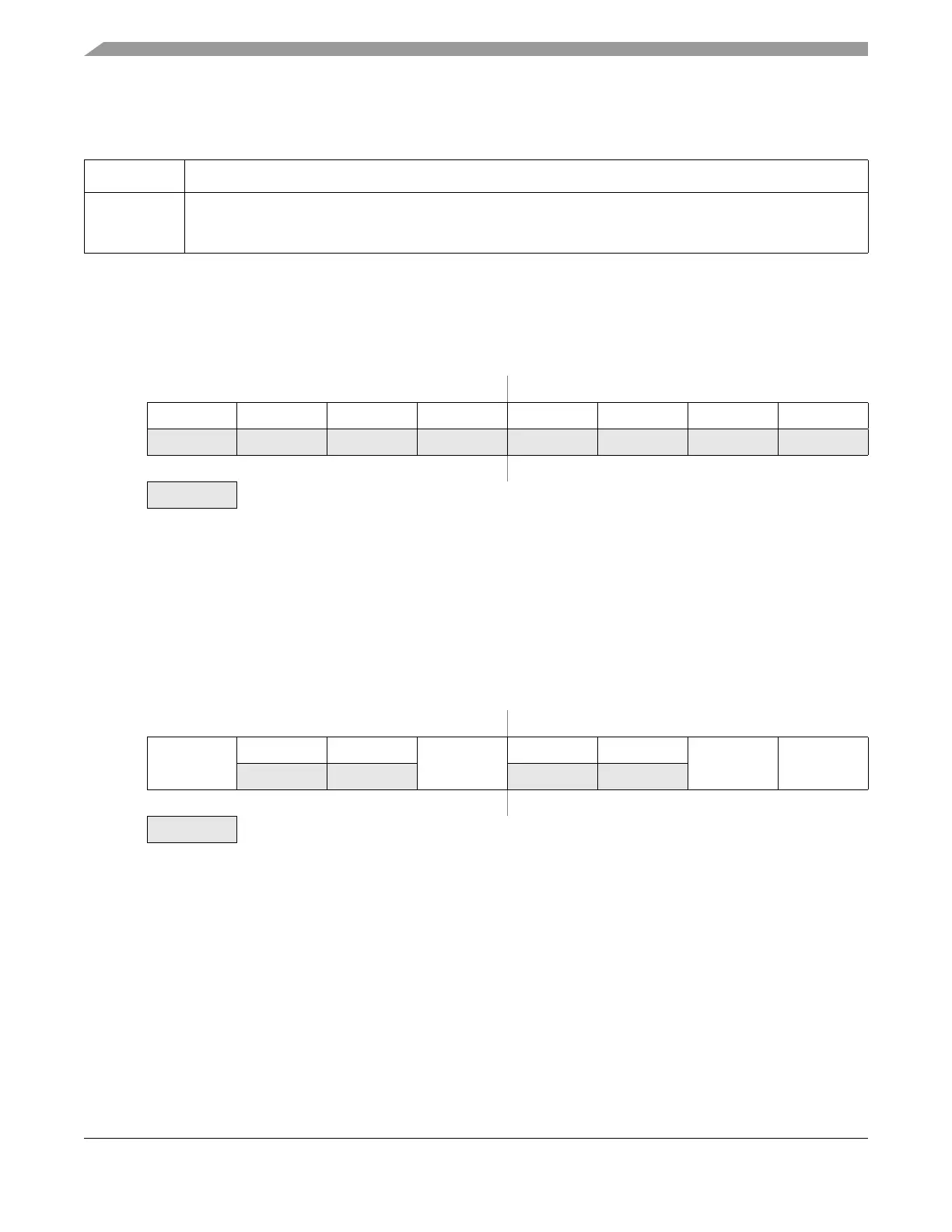
Offset Module Base + 0x000C
76543210
R00000000
W
Reset00000000
= Unimplemented or Reserved
Figure 29-8. Flash Reserved0 Register (FRSV0)
Offset Module Base + 0x0004
76543210
R
CCIE
00
IGNSF
00
FDFD FSFD
W
Reset00000000
= Unimplemented or Reserved
Figure 29-9. Flash Configuration Register (FCNFG)

 Loading...


