Port Integration Module (S12GPIMV1)
MC9S12G Family Reference Manual Rev.1.27
NXP Semiconductors 181
2.4.2 Register Map
The following tables show the individual register maps of groups G1 (Table 2-19), G2 (Table 2-20) and
G3 (Table 2-21).
NOTE
To maintain SW compatibility write data to unimplemented register bits
must be zero.
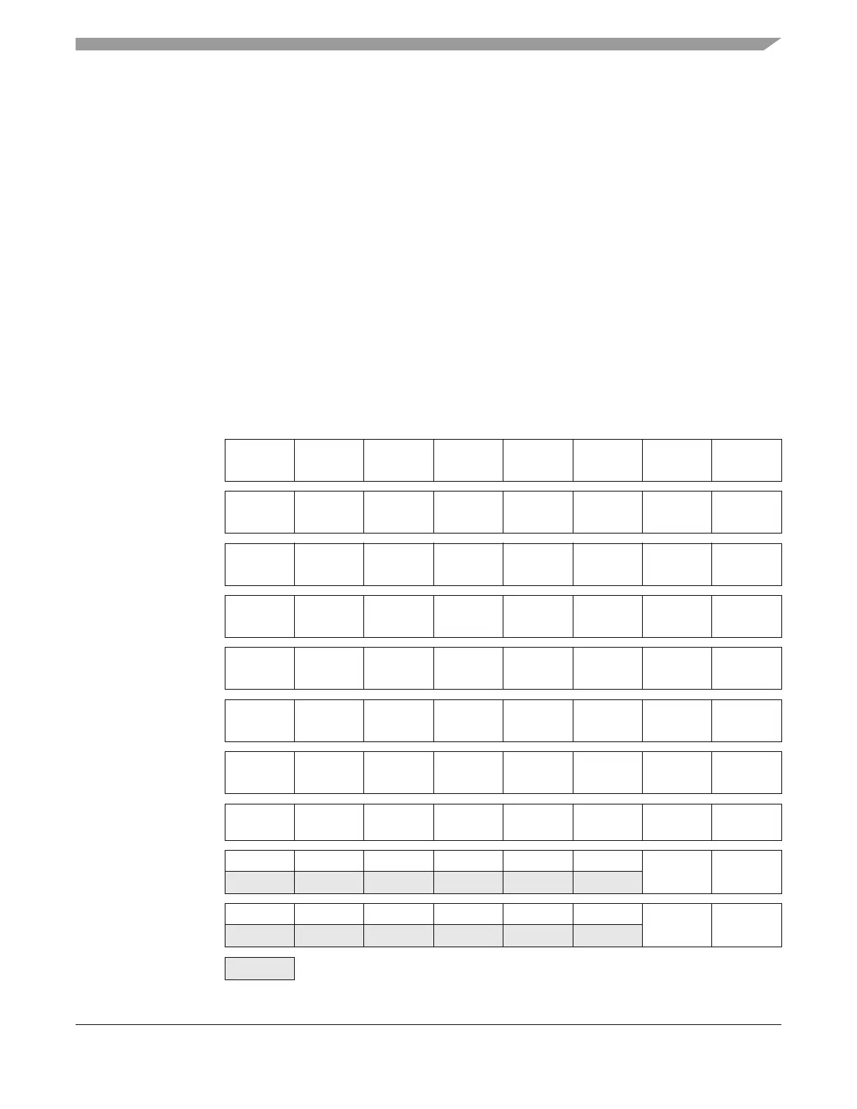
2.4.2.1 Block Register Map (G1)
5
Preset by factory.
6
Routing register only available on G(A)240 and G(A)192 only. Takes only effect if the PKGCR is set to 100 LQFP.
Table 2-19. Block Register Map (G1)
Global Address
Register Name
Bit 7654321Bit 0
0x0000
PORTA
R
PA7 PA6 PA5 PA4 PA3 PA2 PA1 PA0
W
0x0001
PORTB
R
PB7 PB6 PB5 PB4 PB3 PB2 PB1 PB0
W
0x0002
DDRA
R
DDRA7 DDRA6 DDRA5 DDRA4 DDRA3 DDRA2 DDRA1 DDRA0
W
0x0003
DDRB
R
DDRB7 DDRB6 DDRB5 DDRB4 DDRB3 DDRB2 DDRB1 DDRB0
W
0x0004
PORTC
R
PC7PC6PC5PC4PC3PC2PC1PC0
W
0x0005
PORTD
R
PD7PD6PD5PD4PD3PD2PD1PD0
W
0x0006
DDRC
R
DDRC7 DDRC6 DDRC5 DDRC4 DDRC3 DDRC2 DDRC1 DDRC0
W
0x0007
DDRD
R
DDRD7 DDRD6 DDRD5 DDRD4 DDRD3 DDRD2 DDRD1 DDRD0
0x0008
PORTE
R000000
PE1 PE0
W
0x0009
DDRE
R000000
DDRE1 DDRE0
W
= Unimplemented or Reserved

 Loading...


