Electrical Characteristics
MC9S12G Family Reference Manual Rev.1.27
NXP Semiconductors 1211
A.7 NVM
A.7.1 Timing Parameters
The time base for all NVM program or erase operations is derived from the bus clock using the FCLKDIV
register. The frequency of this derived clock must be set within the limits specified as f
NVMOP
. The NVM
module does not have any means to monitor the frequency and will not prevent program or erase operation
at frequencies above or below the specified minimum. When attempting to program or erase the NVM
module at a lower frequency, a full program or erase transition is not assured.
All timing parameters are a function of the bus clock frequency, fNVMBUS. All program and erase times
are also a function of the NVM operating frequency, f
NVMOP
.
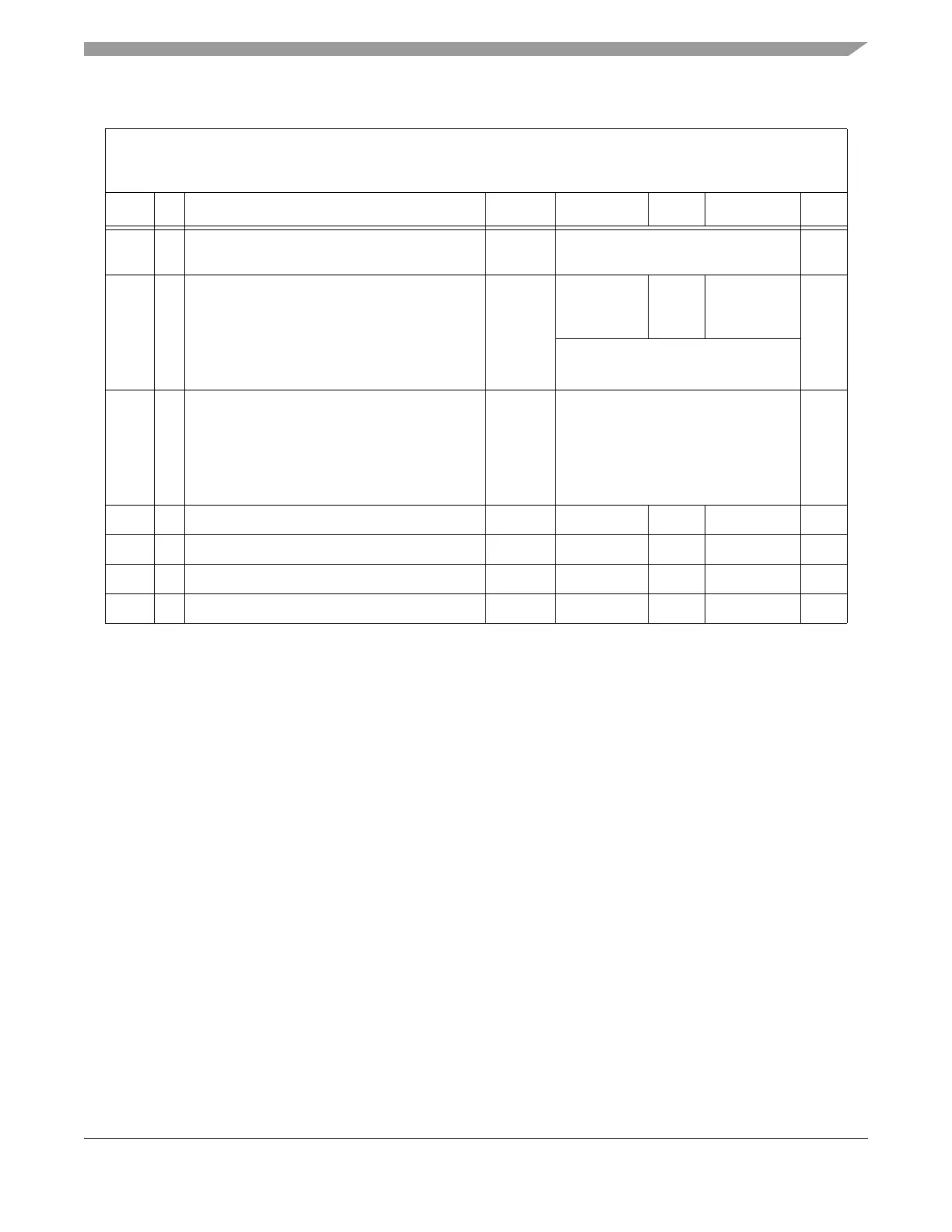
8 C Output Voltage
unbuffered range A or B (load >= 50M)V
out
full DAC Range A or B V
9 P Output Voltage (DRIVE bit = 0)
1
buffered range A (load >= 100K to VSSA)
buffered range A (load >= 100Kto VDDA)
buffered range B (load >= 100K to VSSA)
buffered range B (load >= 100K to VDDA)
V
out
0
0.15
-
-
VDDA-0.15
VDDA V
full DAC Range B
10 P Output Voltage (DRIVE bit = 1)
2
buffered range B with 6.4K load into resistor
divider of 800 /6.56K between VDDA and
VSSA.
(equivalent load is >= 65Kto VSSA) or
(equivalent load is >= 7.5K to VDDA)
V
out
full DAC Range B V
11 D Buffer Output Capacitive load C
load
0 - 100 pF
12 P Buffer Output Offset V
offset
-30 - +30 mV
13 P Settling time t
delay
-35s
14 D Reverence voltage high V
refh
VDDA-0.1V VDDA VDDA+0.1V V
1
DRIVE bit = 1 is not recommended in this case.
2
DRIVE bit = 0 is not allowed with this high load.
Table A-33. Static Electrical Characteristics
Characteristics noted under conditions 3.13V <= VDDA <= 5.5V>, -40°C < Tj < 150°C >, VRH=VDDA, VRL=VSSA
unless otherwise noted. Typical values noted reflect the approximate parameter mean at T
A
= 25°C under nominal
conditions unless otherwise noted.
Num C Ratings Symbol Min Typ Max Unit

 Loading...


