Analog-to-Digital Converter (ADC12B8CV2)
MC9S12G Family Reference Manual Rev.1.27
NXP Semiconductors 435
12.3.2 Register Descriptions
This section describes in address order all the ADC12B8C registers and their individual bits.
12.3.2.1 ATD Control Register 0 (ATDCTL0)
Writes to this register will abort current conversion sequence.
Read: Anytime
Write: Anytime, in special modes always write 0 to Reserved Bit 7.
Module Base + 0x0000
76543210
R
Reserved
000
WRAP3 WRAP2 WRAP1 WRAP0
W
Reset00001111
= Unimplemented or Reserved
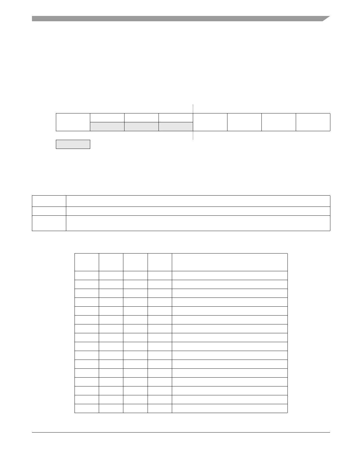
Figure 12-3. ATD Control Register 0 (ATDCTL0)
Table 12-1. ATDCTL0 Field Descriptions
Field Description
3-0
WRAP[3-0]
Wrap Around Channel Select Bits — These bits determine the channel for wrap around when doing
multi-channel conversions. The coding is summarized in Table 12-2.
Table 12-2. Multi-Channel Wrap Around Coding
WRAP3 WRAP2 WRAP1 WRAP0
Multiple Channel Conversions (MULT = 1)
Wraparound to AN0 after Converting
0000 Reserved
1
0001 AN1
0010 AN2
0011 AN3
0100 AN4
0101 AN5
0110 AN6
0111 AN7
1000 AN7
1001 AN7
1010 AN7
1011 AN7
1100 AN7
1101 AN7
1110 AN7
1111 AN7

 Loading...


