Device Overview MC9S12G-Family
MC9S12G Family Reference Manual Rev.1.27
140 NXP Semiconductors
1.9 System Clock Description
For the system clock description please refer to chapter Chapter 1, “Device Overview MC9S12G-Family”.
1.10 Modes of Operation
The MCU can operate in different modes. These are described in 1.10.1 Chip Configuration Summary.
The MCU can operate in different power modes to facilitate power saving when full system performance
is not required. These are described in 1.10.2 Low Power Operation.
Some modules feature a software programmable option to freeze the module status whilst the background
debug module is active to facilitate debugging.
85 PS3 TXD1 — — V
DDX
PERS/PPSS Up
86 PS4 MISO0 — — V
DDX
PERS/PPSS Up
87 PS5 MOSI0 — — V
DDX
PERS/PPSS Up
88 PS6 SCK0 — — V
DDX
PERS/PPSS Up
89 PS7 API_EXTC
LK
SS0
—V
DDX
PERS/PPSS Up
90 VSSX2 — — — — — —
91 VDDX2 — — — — — —
92 PM0 RXCAN — — V
DDX
PERM/PPSM Disabled
93 PM1 TXCAN — — V
DDX
PERM/PPSM Disabled
94PD4———V
DDX
PUCR/PUPDE Disabled
95PD5———V
DDX
PUCR/PUPDE Disabled
96PD6———V
DDX
PUCR/PUPDE Disabled
97PD7———V
DDX
PUCR/PUPDE Disabled
98 PM2 RXD2 — — V
DDX
PERM/PPSM Disabled
99 PM3 TXD2 — — V
DDX
PERM/PPSM Disabled
100 PJ7 KWJ7 SS2
—V
DDX
PERJ/PPSJ Up
1
The regular I/O characteristics (see Section A.2, “I/O Characteristics”) apply if the EXTAL/XTAL function is disabled
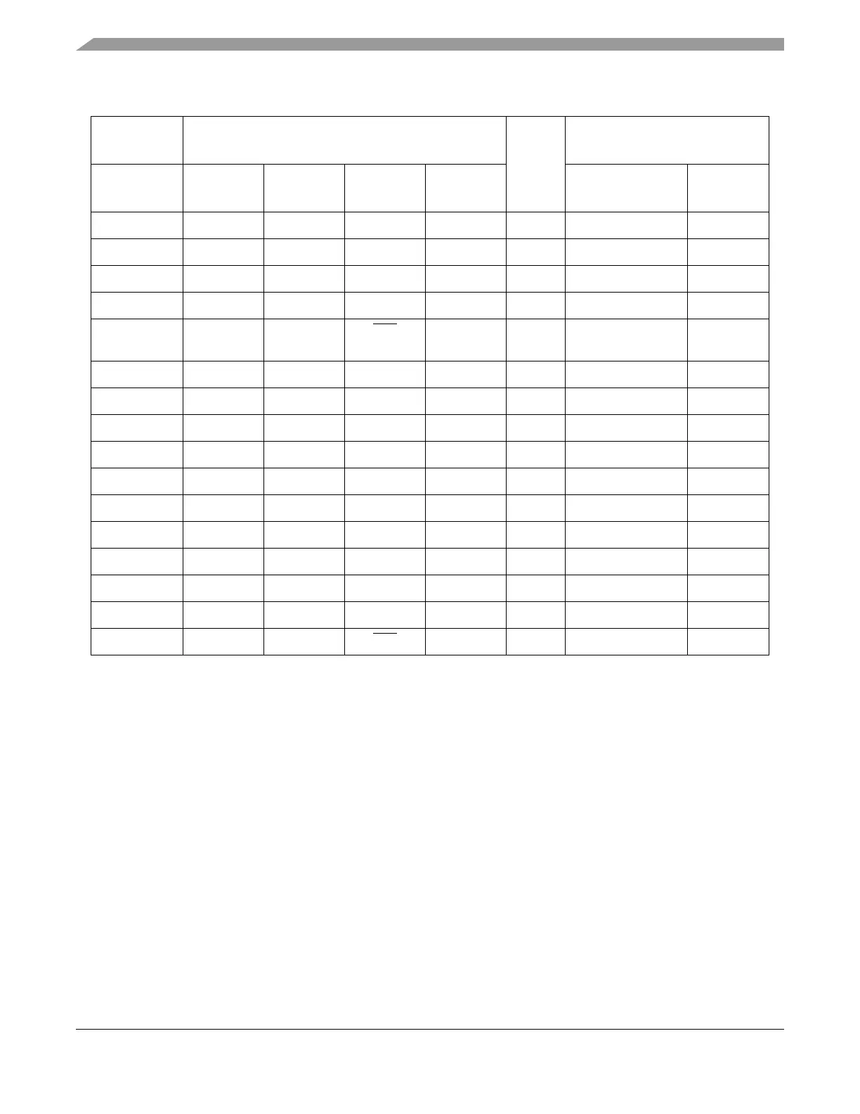
Table 1-32. KGD Option for S12GA192 and S12GA240
Function
<----lowest-----PRIORITY-----highest---->
Power
Supply
Internal Pull
Resistor
Wire Bond
Die Pad
Pin
2nd
Func.
3rd
Func.
4th
Func.
CTRL
Reset
State

 Loading...


