64 KByte Flash Module (S12FTMRG64K1V1)
MC9S12G Family Reference Manual Rev.1.27
924 NXP Semiconductors
Figure 27-3. Memory Controller Resource Memory Map (NVMRES=1)
27.3.2 Register Descriptions
The Flash module contains a set of 20 control and status registers located between Flash module base +
0x0000 and 0x0013.
In the case of the writable registers, the write accesses are forbidden during Fash command execution (for
more detail, see Caution note in Section 27.3).
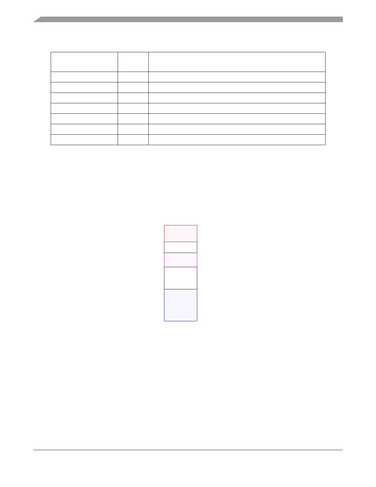
Table 27-6. Memory Controller Resource Fields (NVMRES
1
=1)
1
NVMRES - See Section 27.4.3 for NVMRES (NVM Resource) detail.
Global Address
Size
(Bytes)
Description
0x0_4000 – 0x040FF 256 P-Flash IFR (see Table 27-5)
0x0_4100 – 0x0_41FF 256 Reserved.
0x0_4200 – 0x0_57FF Reserved
0x0_5800 – 0x0_59FF 512 Reserved
0x0_5A00 – 0x0_5FFF 1,536 Reserved
0x0_6000 – 0x0_6BFF 3,072 Reserved
0x0_6C00 – 0x0_7FFF 5,120 Reserved
P-Flash IFR 1 Kbyte (NVMRES=1)
0x0_4000
RAM End = 0x0_59FF
RAM Start = 0x0_5800
Reserved 5120 bytes
Reserved 4608 bytes
0x0_6C00
0x0_7FFF
0x0_4400
Reserved 5k bytes
Reserved 512 bytes

 Loading...


