Background Debug Module (S12SBDMV1)
MC9S12G Family Reference Manual Rev.1.27
NXP Semiconductors 283
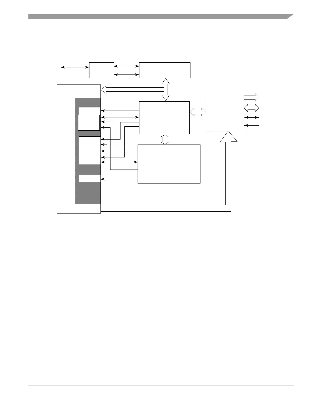
7.1.3 Block Diagram
A block diagram of the BDM is shown in Figure 7-1.
Figure 7-1. BDM Block Diagram
7.2 External Signal Description
A single-wire interface pin called the background debug interface (BKGD) pin is used to communicate
with the BDM system. During reset, this pin is a mode select input which selects between normal and
special modes of operation. After reset, this pin becomes the dedicated serial interface pin for the
background debug mode. The communication rate of this pin is always the BDM clock frequency defined
at device level (refer to device overview section). When modifying the VCO clock please make sure that
the communication rate is adapted accordingly and a communication time-out (BDM soft reset) has
occurred.
7.3 Memory Map and Register Definition
7.3.1 Module Memory Map
Table 7-2 shows the BDM memory map when BDM is active.
16-Bit Shift Register
BKGD
Host
System
Serial
Interface
Data
Control
Register Block
Register
BDMSTS
Instruction Code
and
Execution
Standard BDM Firmware
LOOKUP TABLE
Secured BDM Firmware
LOOKUP TABLE
Bus Interface
and
Control Logic
Address
Data
Control
Clocks
BDMACT
TRACE
ENBDM
SDV
UNSEC

 Loading...


