5V Analog Comparator (ACMPV1)
MC9S12G Family Reference Manual Rev.1.27
NXP Semiconductors 251
3.6 Memory Map and Register Definition
3.6.1 Register Map
Table 3-1 shows the ACMP register map.
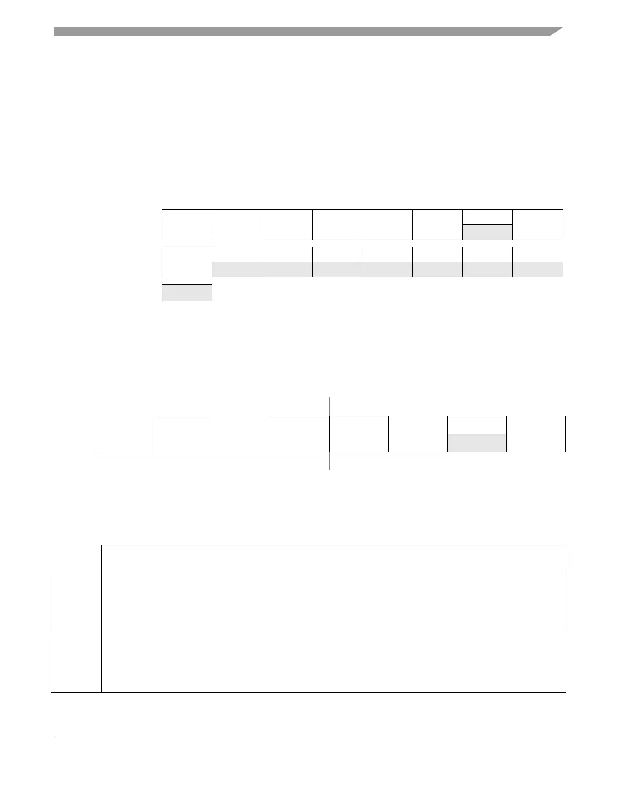
Table 3-1. ACMP Register Map
3.6.2 Register Descriptions
3.6.2.1 ACMP Control Register (ACMPC)
Global Address
Register Name
Bit 7654321Bit 0
0x0260
ACMPC
R
ACIE ACOPE ACICE ACDIEN ACMOD1 ACMOD0
0
ACE
W
0x0261
ACMPS
R
ACIF
ACO000000
W
= Unimplemented or Reserved
Address 0x0260 Access: User read/write
1
1
Read: Anytime
Write: Anytime
76543210
R
ACIE ACOPE ACICE ACDIEN ACMOD1 ACMOD0
0
ACE
W
Reset00000000
Figure 3-3. ACMP Control Register (ACMPC)
Table 3-2. ACMPC Register Field Descriptions
Field Description
7
ACIE
ACMP Interrupt Enable—
Enables the ACMP interrupt.
0 Interrupt disabled
1 Interrupt enabled
6
ACOPE
ACMP Output Pin Enable—
Enables raw comparator output on external ACMPO pin.
0 ACMP output not available
1 ACMP output is driven out on ACMPO

 Loading...


