Serial Communication Interface (S12SCIV5)
MC9S12G Family Reference Manual Rev.1.27
656 NXP Semiconductors
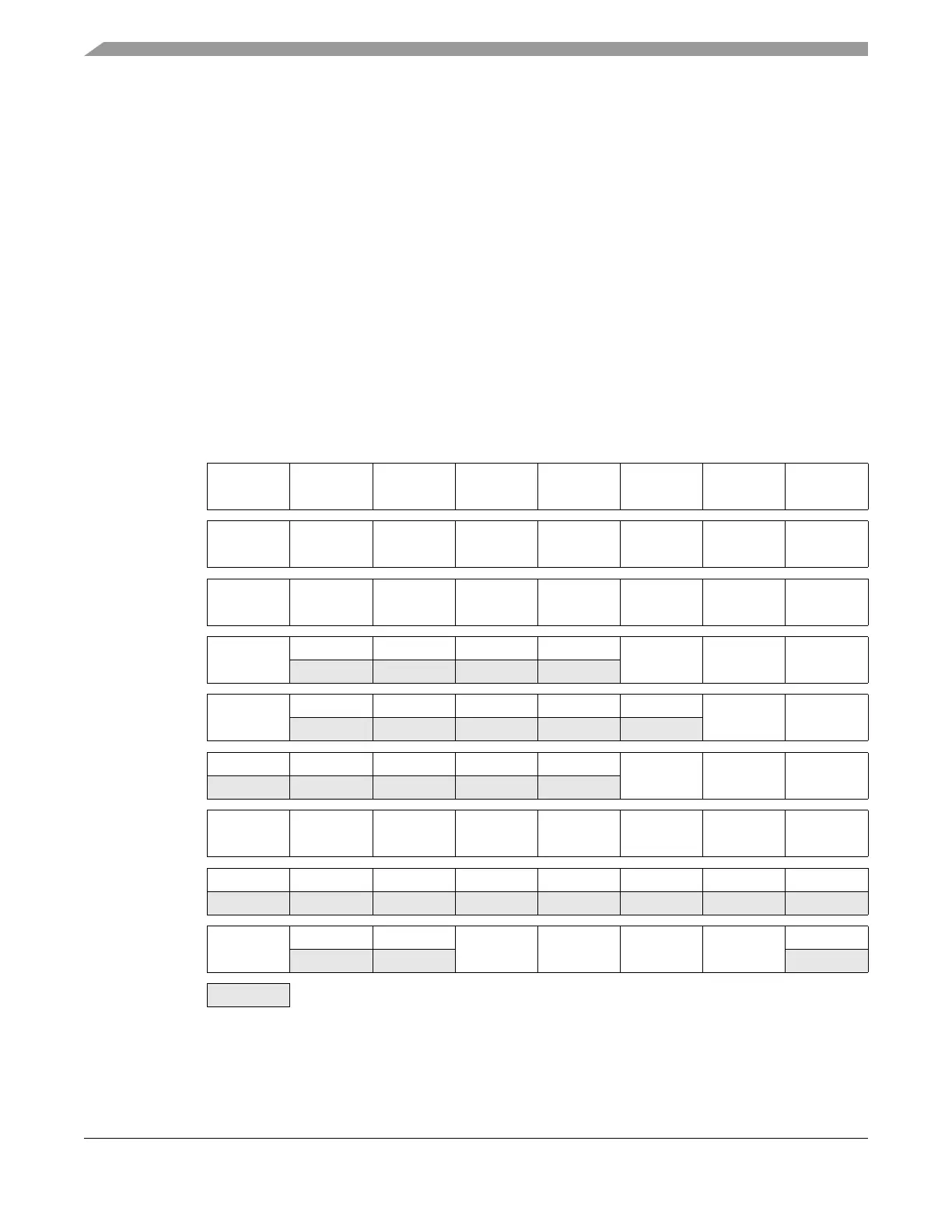
20.3.1 Module Memory Map and Register Definition
The memory map for the SCI module is given below in Figure 20-2. The address listed for each register
is the address offset. The total address for each register is the sum of the base address for the SCI module
and the address offset for each register.
20.3.2 Register Descriptions
This section consists of register descriptions in address order. Each description includes a standard register
diagram with an associated figure number. Writes to a reserved register locations do not have any effect
and reads of these locations return a zero. Details of register bit and field function follow the register
diagrams, in bit order.
Register
Name
Bit 76 5 4 3 2 1Bit 0
0x0000
SCIBDH
1
R
IREN TNP1 TNP0 SBR12 SBR11 SBR10 SBR9 SBR8
W
0x0001
SCIBDL
1
R
SBR7 SBR6 SBR5 SBR4 SBR3 SBR2 SBR1 SBR0
W
0x0002
SCICR1
1
R
LOOPS SCISWAI RSRC M WAKE ILT PE PT
W
0x0000
SCIASR1
2
R
RXEDGIF
0000
BERRV BERRIF BKDIF
W
0x0001
SCIACR1
2
R
RXEDGIE
00000
BERRIE BKDIE
W
0x0002
SCIACR2
2
R0 0 0 0 0
BERRM1 BERRM0 BKDFE
W
0x0003
SCICR2
R
TIE TCIE RIE ILIE TE RE RWU SBK
W
0x0004
SCISR1
R TDRE TC RDRF IDLE OR NF FE PF
W
0x0005
SCISR2
R
AMAP
00
TXPOL RXPOL BRK13 TXDIR
RAF
W
= Unimplemented or Reserved
Figure 20-2. SCI Register Summary (Sheet 1 of 2)

 Loading...


