Electrical Characteristics
MC9S12G Family Reference Manual Rev.1.27
1198 NXP Semiconductors
in an error (10-bit resolution) of less than 1/2 LSB (2.5 mV) at the maximum leakage current. If device or
operating conditions are less than worst case or leakage-induced error is acceptable, larger values of source
resistance of up to 10Kohm are allowed.
A.4.2.4 Source Capacitance
When sampling an additional internal capacitor is switched to the input. This can cause a voltage drop due
to charge sharing with the external and the pin capacitance. For a maximum sampling error of the input
voltage 1LSB (10-bit resilution), then the external filter capacitor, C
f
1024 * (C
INS
–C
INN
).
A.4.2.5 Current Injection
There are two cases to consider.
1. A current is injected into the channel being converted. The channel being stressed has conversion
values of $3FF (in 10-bit mode) for analog inputs greater than V
RH
and $000 for values less than
V
RL
unless the current is higher than specified as disruptive condition.
2. Current is injected into pins in the neighborhood of the channel being converted. A portion of this
current is picked up by the channel (coupling ratio K), This additional current impacts the accuracy
of the conversion depending on the source resistance.
The additional input voltage error on the converted channel can be calculated as:
V
ERR
= K * R
S
* I
INJ
with I
INJ
being the sum of the currents injected into the two pins adjacent to the converted channel.
A.4.3 ADC Accuracy
Table A-21 and Table A-26 specifies the ADC conversion performance excluding any errors due to
current injection, input capacitance and source resistance.
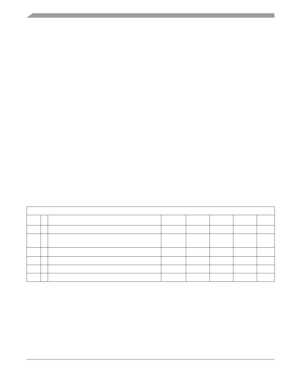
Table A-20. ADC Electrical Characteristics
Supply voltage 3.13 V < V
DDA
< 5.5 V, -40
o
C < T
J
< T
Jmax
1
1
see Table A-4
Num C Rating Symbol Min Typ Max Unit
1 C Max input source resistance
2
2
1 Refer to A.4.2.3 for further information concerning source resistance
R
S
—— 1K
2 D Total input capacitance Non sampling
Total input capacitance Sampling
C
INN
C
INS
—
—
—
—
10
16
pF
3 D Input internal Resistance
R
INA
-515k
4 C Disruptive analog input current I
NA
-2.5 — 2.5 mA
5 C Coupling ratio positive current injection K
p
——1E-4A/A
6 C Coupling ratio negative current injection K
n
——5E-3A/A

 Loading...


