Background Debug Module (S12SBDMV1)
MC9S12G Family Reference Manual Rev.1.27
284 NXP Semiconductors
7.3.2 Register Descriptions
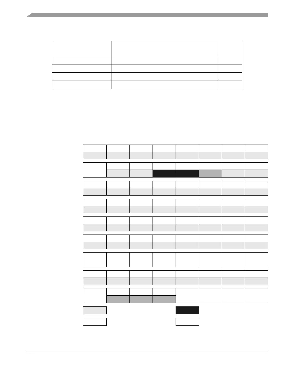
A summary of the registers associated with the BDM is shown in Figure 7-2. Registers are accessed by
host-driven communications to the BDM hardware using READ_BD and WRITE_BD commands.
Table 7-2. BDM Memory Map
Global Address Module
Size
(Bytes)
0x3_FF00–0x3_FF0B BDM registers 12
0x3_FF0C–0x3_FF0E BDM firmware ROM 3
0x3_FF0F Family ID (part of BDM firmware ROM) 1
0x3_FF10–0x3_FFFF BDM firmware ROM 240
Global
Address
Register
Name
Bit 7654321Bit 0
0x3_FF00ReservedRXXXXXX00
W
0x3_FF01 BDMSTS R
ENBDM
BDMACT 0 SDV TRACE 0 UNSEC 0
W
0x3_FF02Reserved RXXXXXXXX
W
0x3_FF03Reserved RXXXXXXXX
W
0x3_FF04ReservedRXXXXXXXX
W
0x3_FF05ReservedRXXXXXXXX
W
0x3_FF06 BDMCCR R
CCR7 CCR6 CCR5 CCR4 CCR3 CCR2 CCR1 CCR0
W
0x3_FF07ReservedR00000000
W
0x3_FF08 BDMPPR R
BPAE
000
BPP3 BPP2 BPP1 BPP0
W
= Unimplemented, Reserved = Implemented (do not alter)
X
= Indeterminate
0
= Always read zero
Figure 7-2. BDM Register Summary

 Loading...


