Digital Analog Converter (DAC_8B5V)
MC9S12G Family Reference Manual Rev.1.27
562 NXP Semiconductors
17.3.4 AMPM Input Pin
This analog pin is used as input for the operational amplifier negative input pin, if the according mode is
selected, see register bit DACM[2:0].
17.4 Memory Map and Register Definition
This sections provides the detailed information of all registers for the DAC_8B5V module.
17.4.1
Register Summary
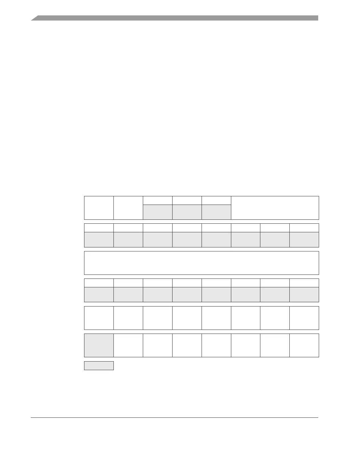
Figure 17-2 shows the summary of all implemented registers inside the
DAC_8B5V
module.
NOTE
Register Address = Module Base Address + Address Offset, where the
Module Base Address is defined at the MCU level and the Address Offset
is defined at the module level.
Address Offset
Register Name
Bit 7654321Bit 0
0x0000
DACCTL
R
FVR DRIVE
000
DACM[2:0]
W
0x0001
Reserved
R00000000
W
0x0002
DACVOL
R
VOLTAGE[7:0]
W
0x0003 - 0x0006
Reserved
R00000000
W
0x0007
Reserved
R
Reserved Reserved Reserved Reserved Reserved Reserved Reserved Reserved
W
0x0007
DACDEBUG
R
0 BUF_EN DAC_EN S3 S2n S2p S1n S1p
W
= Unimplemented
Figure 17-2. DAC_8B5V Register Summaryfv_dac_8b5v_RESERVED

 Loading...


