240 KByte Flash Module (S12FTMRG240K2V1)
MC9S12G Family Reference Manual Rev.1.27
NXP Semiconductors 1133
31.3.2 Register Descriptions
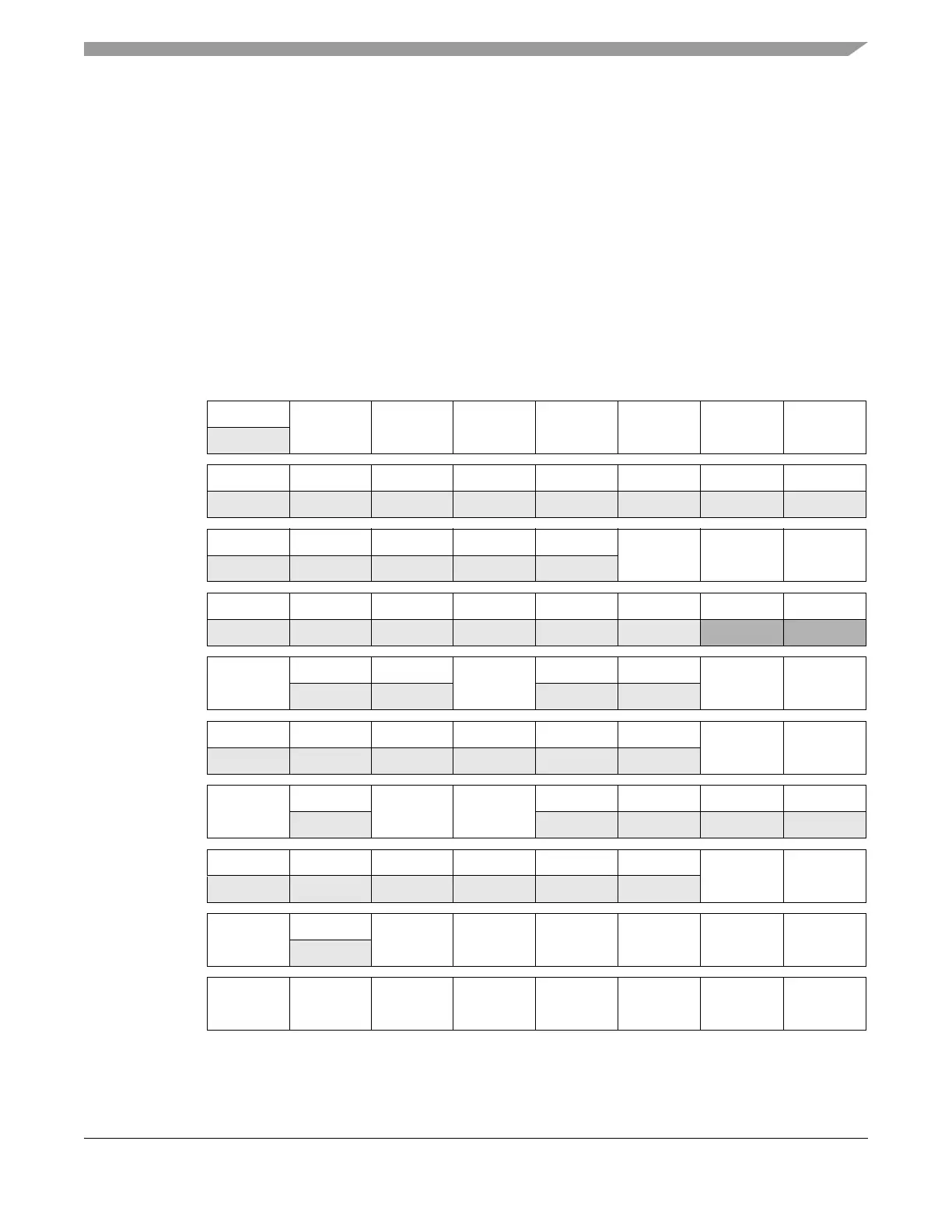
The Flash module contains a set of 20 control and status registers located between Flash module base +
0x0000 and 0x0013.
In the case of the writable registers, the write accesses are forbidden during Fash command execution (for
more detail, see Caution note in Section 31.3).
A summary of the Flash module registers is given in Figure 31-4 with detailed descriptions in the
following subsections.
Address
& Name
76543210
0x0000
FCLKDIV
RFDIVLD
FDIVLCK FDIV5 FDIV4 FDIV3 FDIV2 FDIV1 FDIV0
W
0x0001
FSEC
R KEYEN1 KEYEN0 RNV5 RNV4 RNV3 RNV2 SEC1 SEC0
W
0x0002
FCCOBIX
R0 0 0 0 0
CCOBIX2 CCOBIX1 CCOBIX0
W
0x0003
FRSV0
R00000000
W
0x0004
FCNFG
R
CCIE
00
IGNSF
00
FDFD FSFD
W
0x0005
FERCNFG
R000000
DFDIE SFDIE
W
0x0006
FSTAT
R
CCIF
0
ACCERR FPVIOL
MGBUSY RSVD MGSTAT1 MGSTAT0
W
0x0007
FERSTAT
R000000
DFDIF SFDIF
W
0x0008
FPROT
R
FPOPEN
RNV6
FPHDIS FPHS1 FPHS0 FPLDIS FPLS1 FPLS0
W
0x0009
EEPROT
R
DPOPEN DPS6 DPS5 DPS4 DPS3 DPS2 DPS1 DPS0
W
Figure 31-4. FTMRG240K2 Register Summary

 Loading...


