Device Overview MC9S12G-Family
MC9S12G Family Reference Manual Rev.1.27
NXP Semiconductors 147
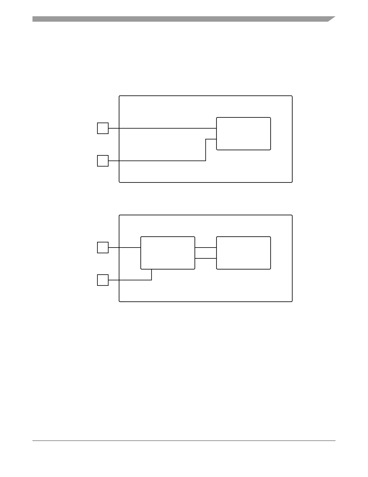
The S12GA192 and the S12GA240 contain a Reference Voltage Attenuator (RVA) module. The
connection of the ADC’s VRH/VRL inputs on these devices is shown in Figure 1-27.
Figure 1-27. ADC VRH/VRL Signal Connection
1.19 BDM Clock Source Connectivity
The BDM clock is mapped to the VCO clock divided by 8.
ADC
VRH
VRL
VRH
VSSA
S12GN16, S12GNA16, S12GN32, S12GNA32, S12GN48, S12G48,
S12GA48, S12G64, S12GA64, S12G96, S12GA96, S12G128,
S12GA128, S12G192, S12G240
ADCRVA
VRH
VRL
VRH_INT
VRL_INT
VSSA
VRHVRH
VSSA
S12GA192, S12GA240

 Loading...


