Pulse-Width Modulator (S12PWM8B8CV2)
MC9S12G Family Reference Manual Rev.1.27
624 NXP Semiconductors
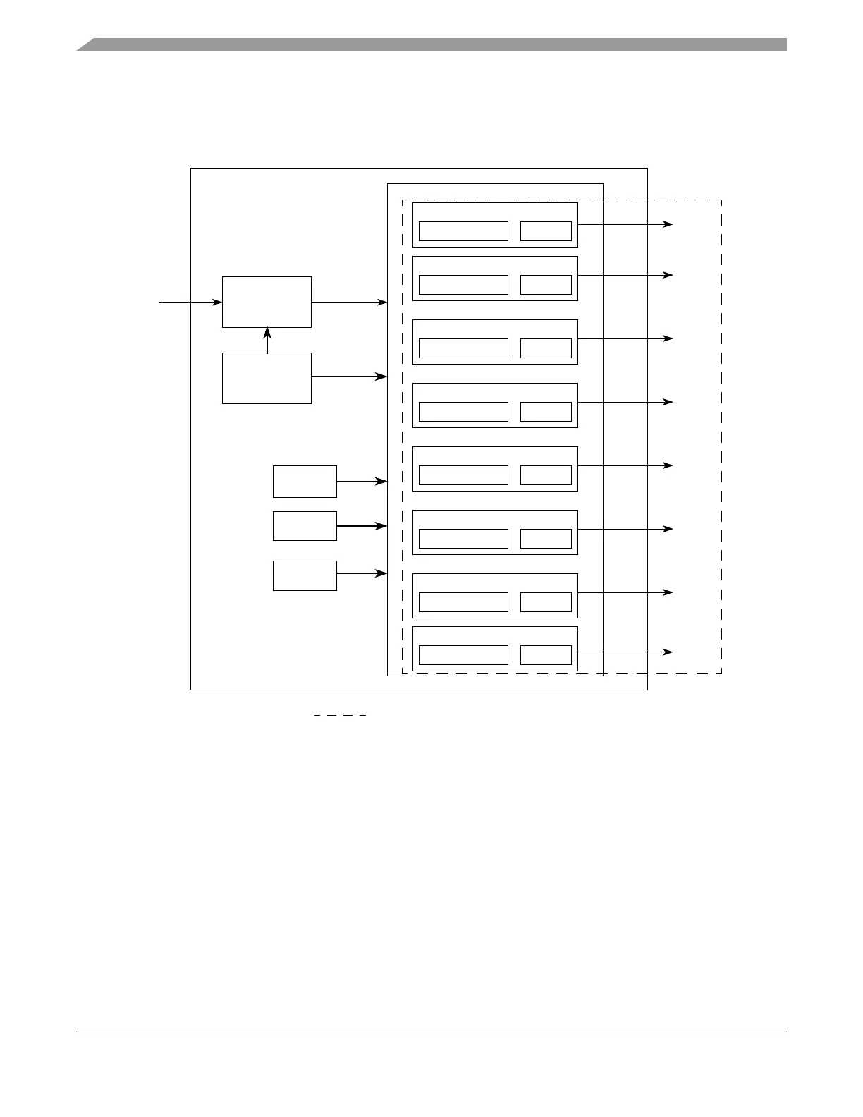
19.1.3 Block Diagram
Figure 19-1 shows the block diagram for the 8-bit up to 8-channel scalable PWM block.
Figure 19-1. Scalable PWM Block Diagram
19.2 External Signal Description
The scalable PWM module has a selected number of external pins. Refer to device specification for exact
number.
19.2.1 PWM7 - PWM0 — PWM Channel 7 - 0
Those pins serve as waveform output of PWM channel 7 - 0.
Period and Duty Counter
Channel 6
Clock Select
PWM Clock
Period and Duty Counter
Channel 5
Period and Duty Counter
Channel 4
Period and Duty Counter
Channel 3
Period and Duty Counter
Channel 2
Period and Duty Counter
Channel 1
Alignment
Polarity
Control
PWM8B8C
PWM6
PWM5
PWM4
PWM3
PWM2
PWM1
Enable
PWM Channels
Period and Duty Counter
Channel 7
Period and Duty Counter
Channel 0
PWM0
PWM7
Bus Clock
Maximum possible channels, scalable in pairs from PWM0 to PWM7.

 Loading...


