Serial Communication Interface (S12SCIV5)
MC9S12G Family Reference Manual Rev.1.27
NXP Semiconductors 655
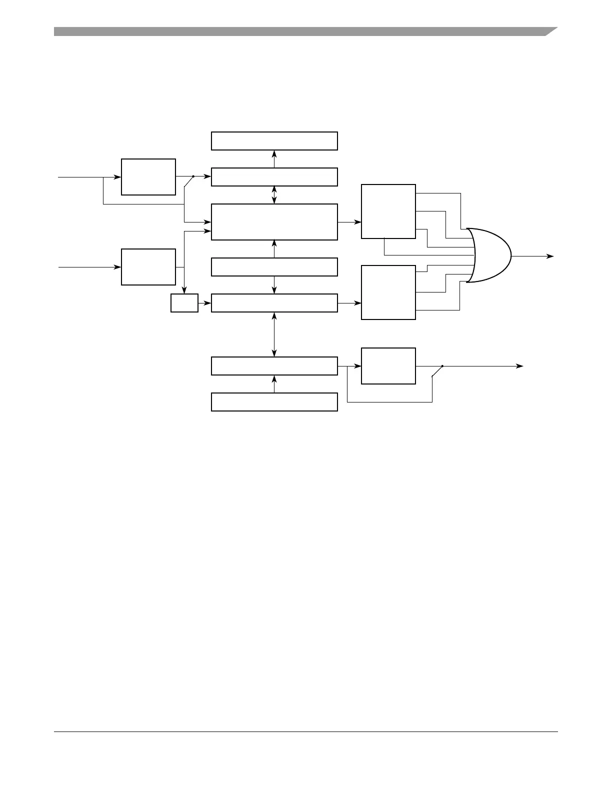
20.1.4 Block Diagram
Figure 20-1 is a high level block diagram of the SCI module, showing the interaction of various function
blocks.
Figure 20-1. SCI Block Diagram
20.2 External Signal Description
The SCI module has a total of two external pins.
20.2.1 TXD — Transmit Pin
The TXD pin transmits SCI (standard or infrared) data. It will idle high in either mode and is high
impedance anytime the transmitter is disabled.
20.2.2 RXD — Receive Pin
The RXD pin receives SCI (standard or infrared) data. An idle line is detected as a line high. This input is
ignored when the receiver is disabled and should be terminated to a known voltage.
20.3 Memory Map and Register Definition
This section provides a detailed description of all the SCI registers.
SCI Data Register
RXD Data In
Data Out TXD
Receive Shift Register
Infrared
Decoder
Receive & Wakeup
Control
Data Format Control
Transmit Control
Baud Rate
Generator
Bus Clock
1/16
Transmit Shift Register
SCI Data Register
Receive
Interrupt
Generation
Transmit
Interrupt
Generation
Infrared
Encoder
IDLE
RDRF/OR
TC
TDRE
BRKD
BERR
RXEDG
SCI
Interrupt
Request

 Loading...


