Port Integration Module (S12GPIMV1)
MC9S12G Family Reference Manual Rev.1.27
178 NXP Semiconductors
2.4 PIM Ports - Memory Map and Register Definition
This section provides a detailed description of all PIM registers.
2.4.1 Memory Map
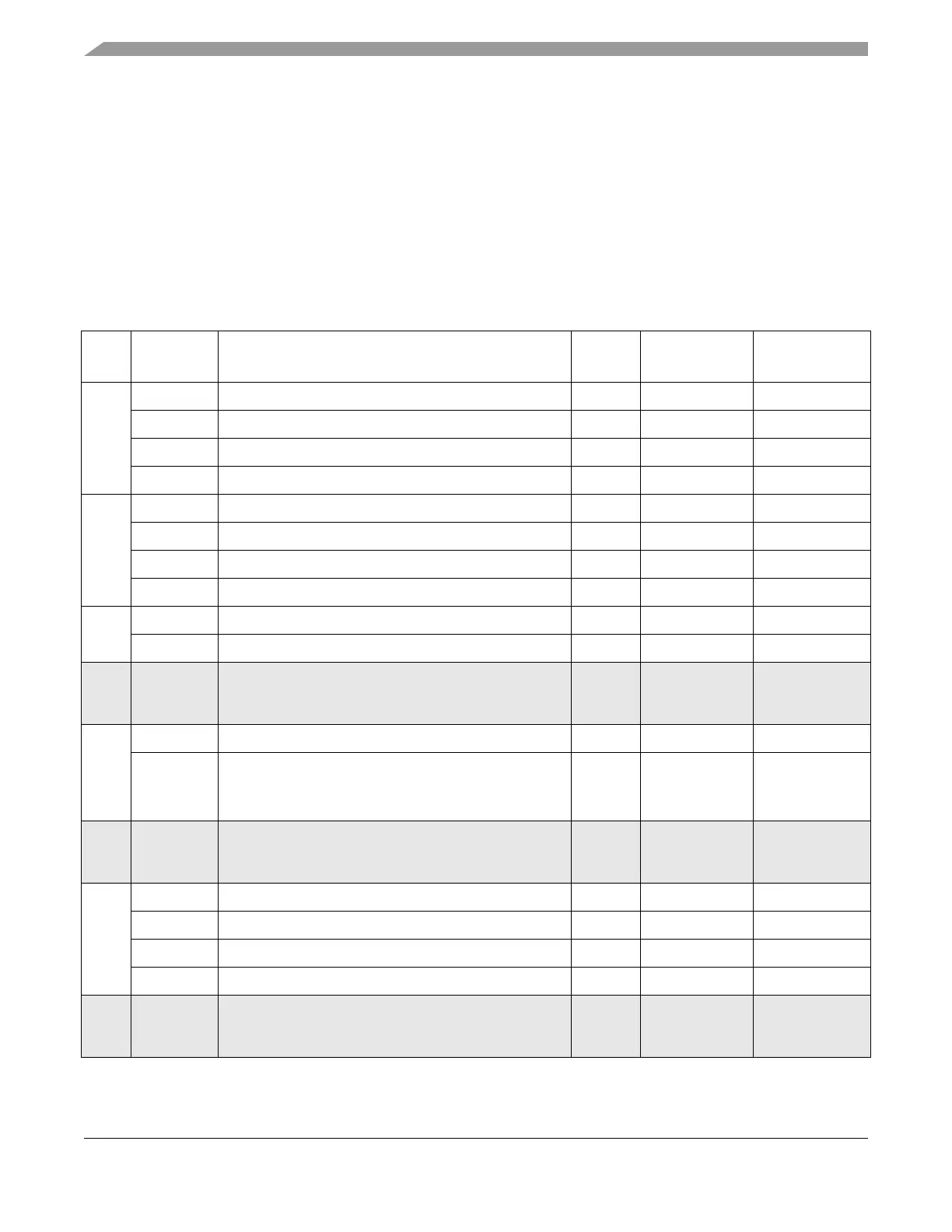
Table 2-18 shows the memory maps of all groups (for definitions see Table 2-2). Addresses 0x0000 to
0x0007 are only implemented in group G1 otherwise reserved.
Table 2-18. Block Memory Map (0x0000-0x027F)
Port
Global
Address
Register Access Reset Value Section/Page
(A)
(B)
0x0000 PORTA—Port A Data Register
1
R/W 0x00 2.4.3.1/2-197
0x0001 PORTB—Port B Data Register
1
R/W 0x00 2.4.3.2/2-197
0x0002 DDRA—Port A Data Direction Register
1
R/W 0x00 2.4.3.3/2-198
0x0003 DDRB—Port B Data Direction Register
1
R/W 0x00 2.4.3.4/2-199
(C)
(D)
0x0004 PORTC—Port C Data Register
1
R/W 0x00 2.4.3.5/2-199
0x0005 PORTD—Port D Data Register
1
R/W 0x00 2.4.3.6/2-200
0x0006 DDRC—Port C Data Direction Register
1
R/W 0x00 2.4.3.7/2-201
0x0007 DDRD—Port D Data Direction Register
1
R/W 0x00 2.4.3.8/2-201
E 0x0008 PORTE—Port E Data Register R/W 0x00
0x0009 DDRE—Port E Data Direction Register R/W 0x00
0x000A
:
0x000B
Non-PIM address range
2
- - -
(A)
(B)
(C)
(D)
E
0x000C PUCR—Pull Control Register R/W 0x50 2.4.3.11/2-203
0x000D Reserved R 0x00
0x000E
:
0x001B
Non-PIM address range
2
- - -
0x001C ECLKCTL—ECLK Control Register R/W 0xC0 2.4.3.12/2-205
0x001D Reserved R 0x00
0x001E IRQCR—IRQ Control Register R/W 0x00 2.4.3.13/2-205
0x001F Reserved R 0x00
0x0020
:
0x023F
Non-PIM address range
2
- - -

 Loading...


