Port Integration Module (S12GPIMV1)
MC9S12G Family Reference Manual Rev.1.27
198 NXP Semiconductors
2.4.3.3 Port A Data Direction Register (DDRA)
1
Read: Anytime. The data source is depending on the data direction value.
Write: Anytime
Table 2-23. PORTB Register Field Descriptions
Field Description
7-0
PB
Port B general-purpose input/output data—Data Register
The associated pin can be used as general-purpose I/O. In general-purpose output mode the port data register bit
value is driven to the pin.
If the associated data direction bit is set to 1, a read returns the value of the port data register bit, otherwise the
buffered pin input state is read.
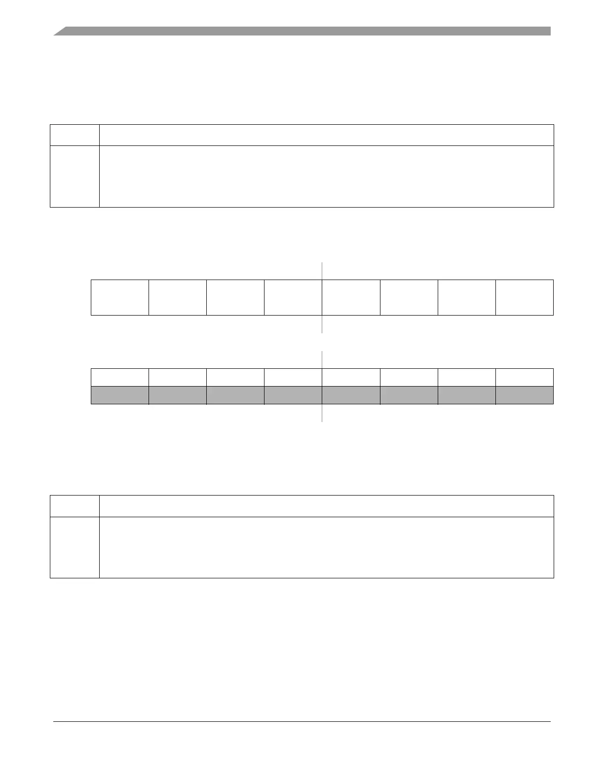
Address 0x0002 (G1) Access: User read/write
1
1
Read: Anytime
Write: Anytime
76543210
R
DDRA7 DDRA6 DDRA5 DDRA4 DDRA3 DDRA2 DDRA1 DDRA0
W
Reset00000000
Address 0x0002 (G2, G3) Access: User read only
76543210
R00000000
W
Reset00000000
Figure 2-4. Port A Data Direction Register (DDRA)
Table 2-24. DDRA Register Field Descriptions
Field Description
7-0
DDRA
Port A Data Direction—
This bit determines whether the associated pin is an input or output.
1 Associated pin configured as output
0 Associated pin configured as input

 Loading...


