Electrical Characteristics
MC9S12G Family Reference Manual Rev.1.27
1208 NXP Semiconductors
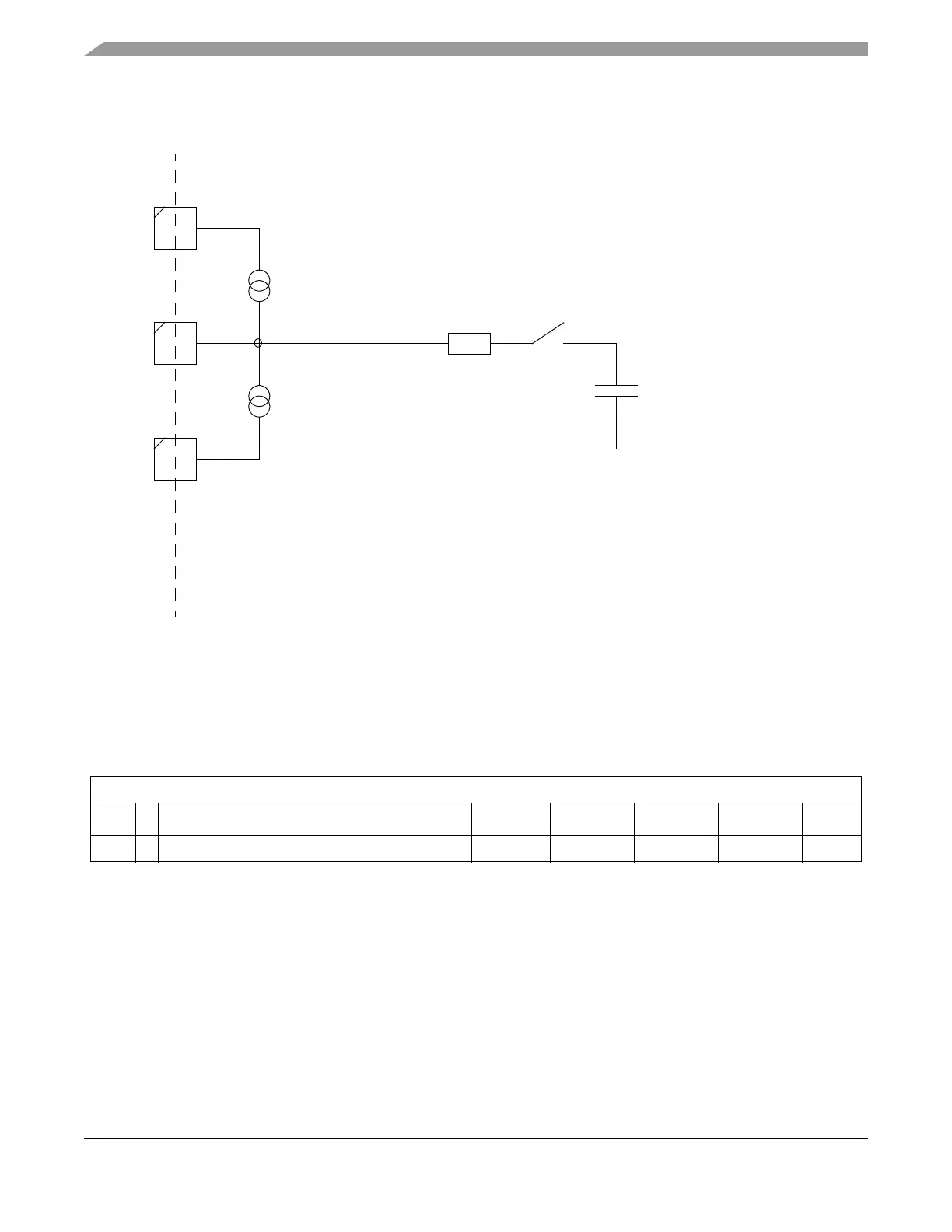
A.4.3.2 ADC Analog Input Parasitics
Figure A-2. ADC Analog Input Parasitics
A.4.4 ADC Temperature Sensor
Table A-30. ADC Temperature Sensor
A.5 ACMP Characteristics
This section describes the electrical characteristics of the analog comparator.
Num C Rating Symbol Min Typ Max Unit
1 T Temperature Sensor Slope dV
TS
-4.0 -3.8 -3.6 mV/C
PAD00-
PAD11
VDDA
VSSA
T
jmax
=130
o
C
I
leakp
< 0.5
A
I
leakn
< 0.5
A
C
bottom
3.7pF < S/H Cap < 6.2pF
(incl parasitics)
920
< R
path
< 9.9K
(incl parasitics)
sampling time is 4 to 24 adc clock cycles of
0.25MHz to 8MHz -> 96
s >= tsample >= 500ns
Switch resistance depends on input voltage, corner ranges are shown.
Leakage current is guaranteed by specification.
Complete 10bit conversion takes between 19 and 41 adc clock cycles
connected to low ohmic
supply during sampling
C
top
C
top
potential just prior to sampling is either
a) ~ last converted channel potential or
b) ground level if S/H discharge feature is enabled.
 Loading...