Electrical Characteristics
MC9S12G Family Reference Manual Rev.1.27
NXP Semiconductors 1207
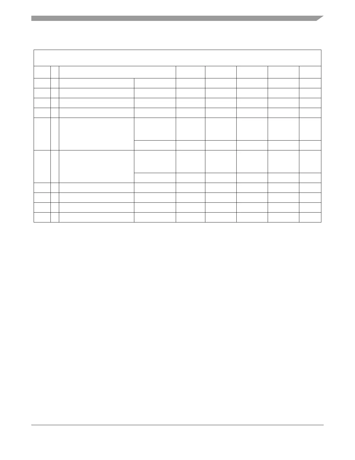
Table A-29. ADC Conversion Performance 5V range, RVA enabled
Supply voltage V
DDA
=5.0 V, -40
o
C < T
J
< 150
o
C. V
RH
= 5.0V. f
ADCCLK
= 0.25 .. 2MHz
1
The values are tested to be valid with no port AD/C output drivers switching simultaneous with conversions.
1
Upper limit of f
ADCCLK
is restricted when RVA attenuation mode is engaged.
Num C Rating Symbol Min Typ Max Unit
1 P Resolution 12-Bit LSB 0.61 mV
2 P Differential Nonlinearity 12-Bit DNL 3 4 counts
3 P Integral Nonlinearity 12-Bit INL 3.5 5 counts
4 C Absolute Error
2
2
These values include the quantization error which is inherently 1/2 count for any A/D converter and the error of the internally
generated reference values..
12-Bit AE 8 counts
5 P internal VRH reference voltage LQFP48,
LQFP64,
LQFP100
Vvrh_int 4.495 4.505 V
KGD Vvrh_int 4.490 4.510 V
6 P internal VRL reference voltage LQFP48,
LQFP64,
LQFP100
Vvrh_int 1.995 2.005V V
KGD Vvrl_int 1.990 2.010V V
7 C VRH_INT drift vs temperature
3
3
Please note: although different in value, drift of vrh_int and vrl_int will go in the same direction.
Vvrh_drift -2 2 mV
8 C VRL_INT drift vs temperature Vvrl_drift -2.5 2.5 mV
9 C rva turn on settling time t
settling_on
2.5 s
10 C rva turn off settling time t
settling_off
1 s

 Loading...


