Port Integration Module (S12GPIMV1)
MC9S12G Family Reference Manual Rev.1.27
196 NXP Semiconductors
2.4.3 Register Descriptions
This section describes the details of all configuration registers. Every register has the same functionality
in all groups if not specified separately. Refer to the register figures for reserved locations. If not stated
differently, writing to reserved bits has not effect and read returns zero.
NOTE
• All register read accesses are synchronous to internal clocks
• General-purpose data output availability depends on prioritization;
input data registers always reflect the pin status independent of the use
• Pull-device availability, pull-device polarity, wired-or mode,
key-wakeup functionality are independent of the prioritization unless
noted differently in section Section 2.3, “PIM Routing - Functional
description”.
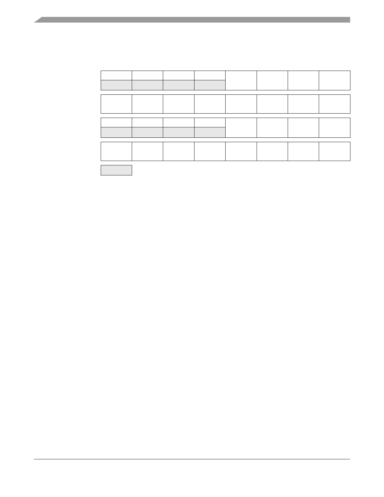
0x027C
PIE0AD
R0000
PIE0AD3 PIE0AD2 PIE0AD1 PIE0AD0
W
0x027D
PIE1AD
R
PIE1AD7 PIE1AD6 PIE1AD5 PIE1AD4 PIE1AD3 PIE1AD2 PIE1AD1 PIE1AD0
W
0x027E
PIF0AD
R0000
PIF0AD3 PIF0AD2 PIF0AD1 PIF0AD0
W
0x027F
PIF1AD
R
PIF1AD7 PIF1AD6 PIF1AD5 PIF1AD4 PIF1AD3 PIF1AD2 PIF1AD1 PIF1AD0
W
Table 2-21. Block Register Map (G3) (continued)
Global Address
Register Name
Bit 7654321Bit 0
= Unimplemented or Reserved

 Loading...


