Electrical Characteristics
MC9S12G Family Reference Manual Rev.1.27
1210 NXP Semiconductors
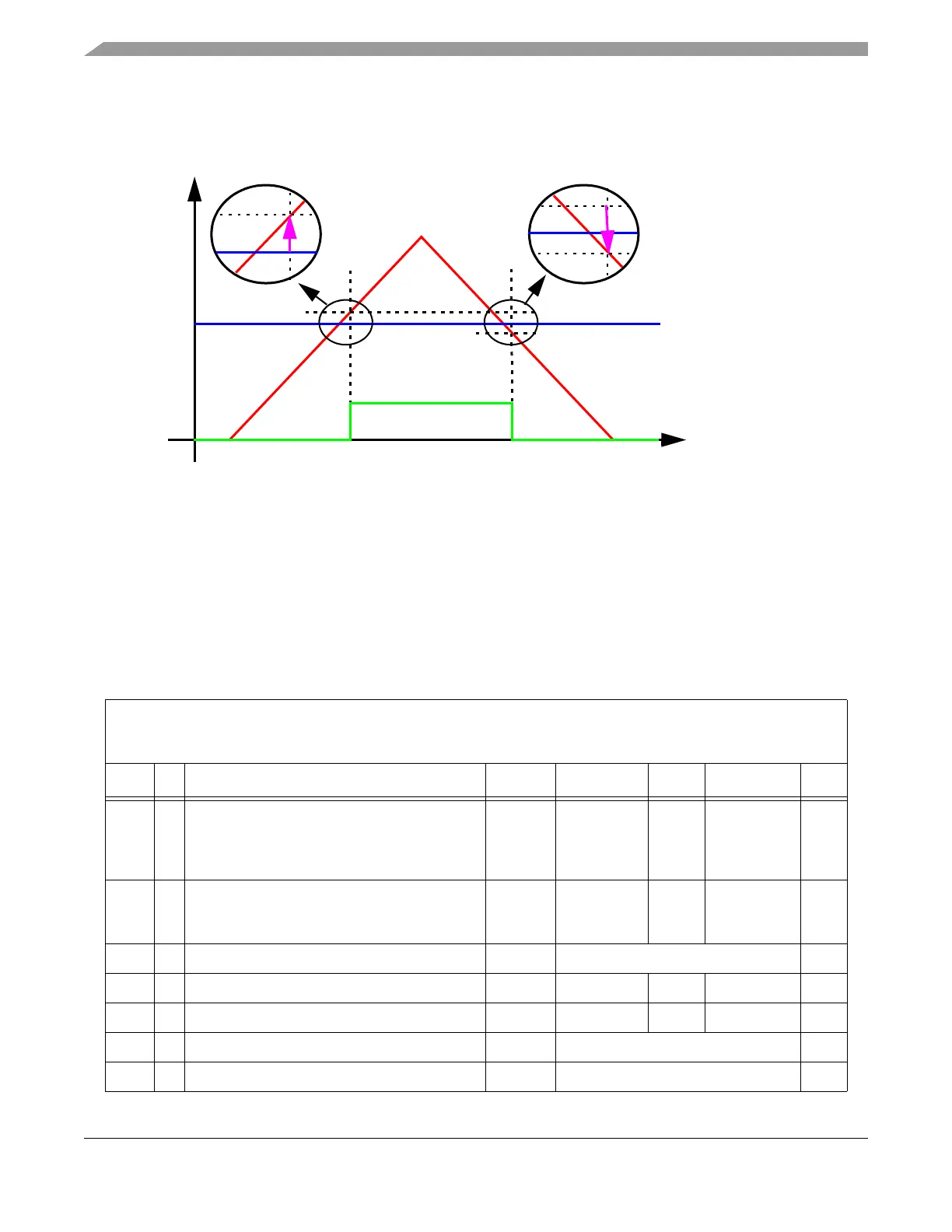
Figure A-3. Input Offset and Hysteresis
A.6 DAC Characteristics
This section describes the electrical characteristics of the digital to analog converter.
Table A-33. Static Electrical Characteristics
Characteristics noted under conditions 3.13V <= VDDA <= 5.5V>, -40°C < Tj < 150°C >, VRH=VDDA, VRL=VSSA
unless otherwise noted. Typical values noted reflect the approximate parameter mean at T
A
= 25°C under nominal
conditions unless otherwise noted.
Num C Ratings Symbol Min Typ Max Unit
1
D
P
P
Supply Current
buffer disabled
buffer enabled FVR=0 DRIVE=1
buffer enabled FVR=1 DRIVE=0
I
buf
-
-
-
-
365
215
5
800
800
A
2
D
P
Reference current
reference disabled
reference enabled
I
ref
--
50
1
150
A
3 D Resolution 8 bit
4 C Relative Accuracy @ amplifier output INL -0.5 +0.5 LSB
5 P Differential Nonlinearity @ amplifier output DNL -0.5 +0.5 LSB
6 D DAC Range A (FVR bit = 1) V
out
0...255/256(VRH-VRL)+VRL V
7 D DAC Range B (FVR bit = 0 V
out
32...287/320(VRH-VRL)+VRL V
Offset
Hysteresis
ACMPM
ACMPP
ACMPO
V
t

 Loading...


