Serial Peripheral Interface (S12SPIV5)
MC9S12G Family Reference Manual Rev.1.27
712 NXP Semiconductors
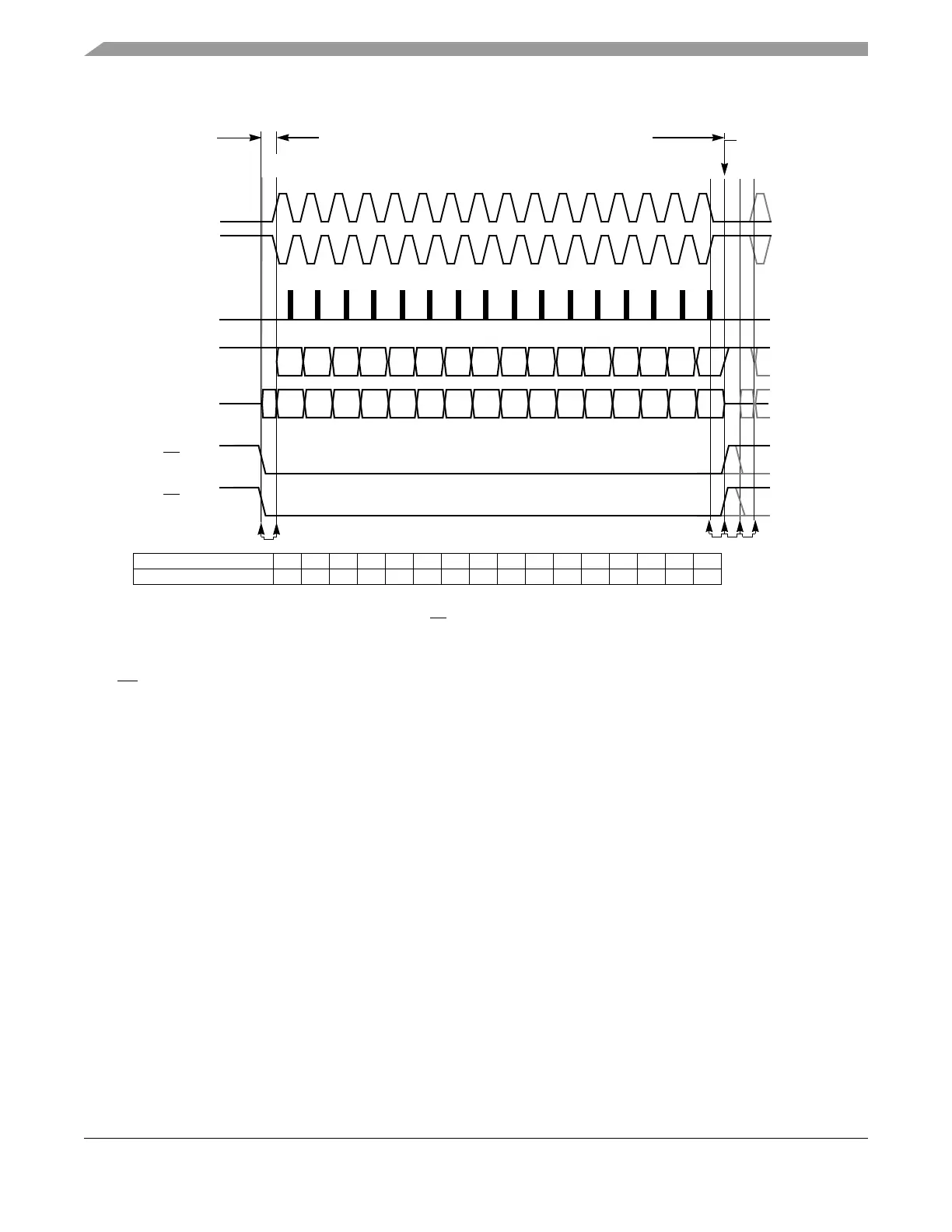
Figure 21-15. SPI Clock Format 1 (CPHA = 1), with 16-Bit Transfer Width selected (XFRW = 1)
The SS line can remain active low between successive transfers (can be tied low at all times). This format
is sometimes preferred in systems having a single fixed master and a single slave that drive the MISO data
line.
• Back-to-back transfers in master mode
In master mode, if a transmission has completed and new data is available in the SPI data register,
this data is sent out immediately without a trailing and minimum idle time.
The SPI interrupt request flag (SPIF) is common to both the master and slave modes. SPIF gets set one
half SCK cycle after the last SCK edge.
21.4.4 SPI Baud Rate Generation
Baud rate generation consists of a series of divider stages. Six bits in the SPI baud rate register (SPPR2,
SPPR1, SPPR0, SPR2, SPR1, and SPR0) determine the divisor to the SPI module clock which results in
the SPI baud rate.
The SPI clock rate is determined by the product of the value in the baud rate preselection bits
(SPPR2–SPPR0) and the value in the baud rate selection bits (SPR2–SPR0). The module clock divisor
equation is shown in Equation 21-3.
t
L
Begin End
SCK (CPOL = 0)
SAMPLE I
CHANGE O
SEL SS
(O)
Transfer
SCK (CPOL = 1)
MSB first (LSBFE = 0)
LSB first (LSBFE = 1)
MSB
LSB
LSB
MSB
Bit 13
Bit 2
Bit 14
Bit 1
Bit 12
Bit 3
Bit 11
Bit 4
Bit 5
CHANGE O
SEL SS
(I)
MOSI pin
MISO pin
Master only
MOSI/MISO
t
T
If next transfer begins here
for t
T
, t
l
, t
L
Minimum 1/2 SCK
t
I
t
L
t
L
= Minimum leading time before the first SCK edge, not required for back-to-back transfers
t
T
= Minimum trailing time after the last SCK edge
t
I
= Minimum idling time between transfers (minimum SS high time), not required for back-to-back transfers
1
2
3
4
5
6
7
8
9
10
11
12
13
14
15
16
SCK Edge Number
End of Idle State Begin of Idle State
17
18
19
20
21
22
23
24
25
26
27
28
29
30
31
32
Bit 10Bit 9Bit 8Bit 7Bit 6 Bit 4 Bit 3 Bit 2 Bit 1
Bit 6Bit 5 Bit 7 Bit 8 Bit 9 Bit 10Bit 11 Bit 12Bit 13Bit 14

 Loading...


