Detailed Register Address Map
MC9S12G Family Reference Manual Rev.1.27
NXP Semiconductors 1233
Appendix B
Detailed Register Address Map
Revision History
B.1 Detailed Register Map
The following tables show the detailed register map of the MC9S12G-Family.
NOTE
This is a summary of all register bits implemented on MC9S12G devices.
Each member of the MC9S12G-Family implements the subset of registers,
which is associated with its feature set (see Table 1-1).
Version
Number
Revision
Date
Description of Changes
Rev 0.05 30-Aug-2010 • Updated ADCCTL2 register in Appendix B, “Detailed Register Address Map”.
• Updated CPMUOSC register in Appendix B, “Detailed Register Address Map”.
Rev 0.06 18-Oct-2010 • Updated ADC registers in Appendix B, “Detailed Register Address Map”.
Rev 0.07 9-Nov-2010 • Updated CPMU registers in Appendix B, “Detailed Register Address Map”.
Rev 0.08 4-Dec-2010 • Updated PIM registers in Appendix B, “Detailed Register Address Map”.
Rev 0.09 24-Apr-2012 • Typos and formatting
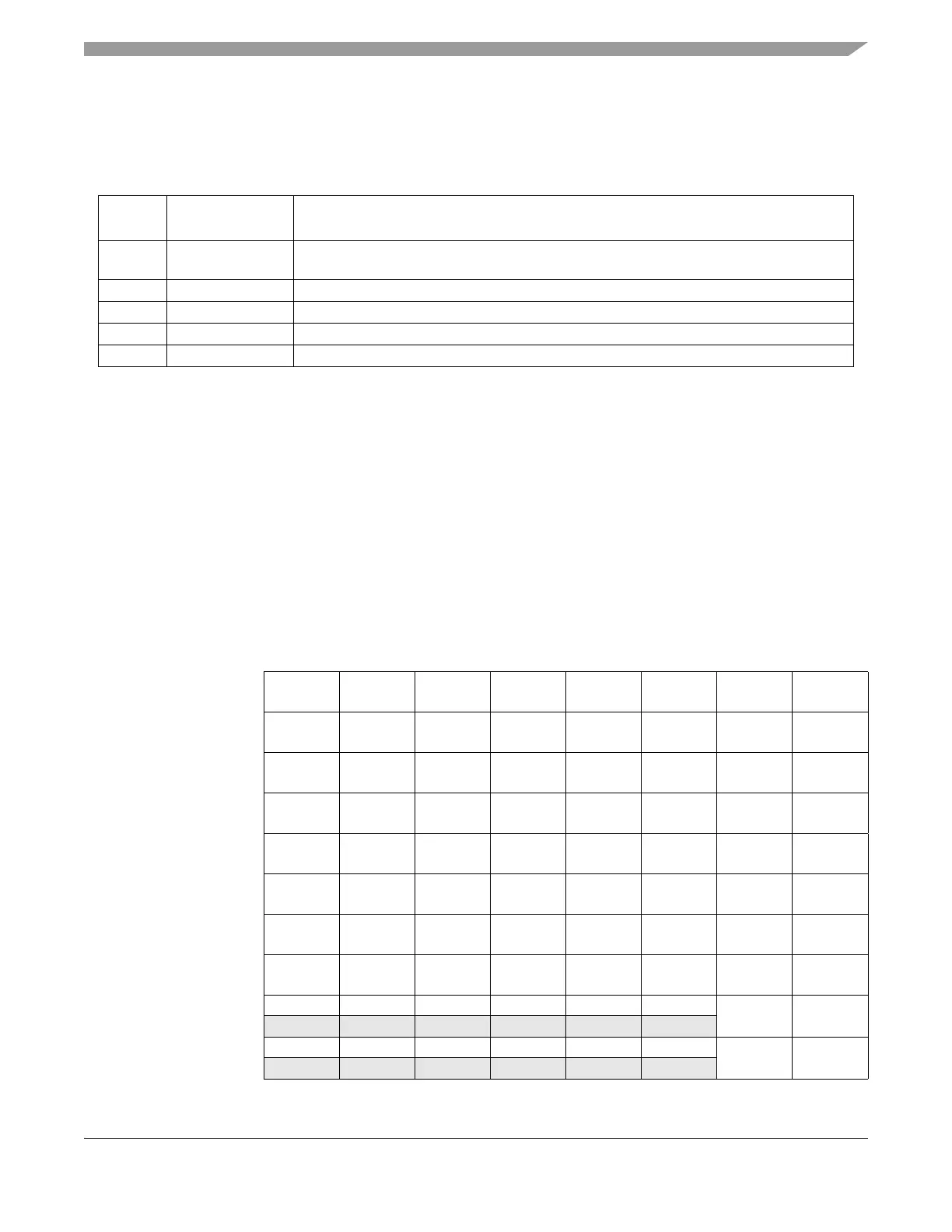
0x0000–0x0009 Port Integration Module (PIM) Map 1 of 6
Address Name Bit 7 Bit 6 Bit 5 Bit 4 Bit 3 Bit 2 Bit 1 Bit 0
0x0000 PORTA
R
PA7PA6PA5PA4PA3PA2PA1PA 0
W
0x0001 PORTB
R
PB7 PB6 PB5 PB4 PB3 PB2 PB1 PB0
W
0x0002 DDRA
R
DDRA7 DDRA6 DDRA5 DDRA4 DDRA3 DDRA2 DDRA1 DDRA0
W
0x0003 DDRB
R
DDRB7 DDRB6 DDRB5 DDRB4 DDRB3 DDRB2 DDRB1 DDRB0
W
0x0004 PORTC
R
PC7 PC6 PC5 PC4 PC3 PC2 PC1 PC0
W
0x0005 PORTD
R
PD7 PD6 PD5 PD4 PD3 PD2 PD1 PD0
W
0x0006 DDRC
R
DDRC7 DDRC6 DDRC5 DDRC4 DDRC3 DDRC2 DDRC1 DDRC0
W
0x0007 DDRD
R
DDRD7 DDRD6 DDRD5 DDRD4 DDRD3 DDRD2 DDRD1 DDRD0
W
0x0008 PORTE
R000000
PE1 PE0
W
0x0009 DDRE
R000000
DDRE1 DDRE0
W

 Loading...


