Device Overview MC9S12G-Family
MC9S12G Family Reference Manual Rev.1.27
NXP Semiconductors 45
1.7 Signal Description and Device Pinouts
This section describes signals that connect off-chip. It includes a pinout diagram, a table of signal
properties, and detailed discussion of signals. It is built from the signal description sections of the
individual IP blocks on the device.
1.7.1 Pin Assignment Overview
Table 1-6 provides a summary of which ports are available for each package option.
MC9S12GNA16
0N48A 0xF380
0N57V 0xF380
MC9S12GN16
0N48A
3
0xF380
3
0N57V
3
0xF380
3
1N48A
4
0xF381
4
1N57V
4
0xF381
4
1
Only available in 48-pin LQFP and 64-pin LQFP
2
Only available in 32-pin LQFP
3
Only available in 48-pin LQFP and 48-pin QFN
4
Only available in 20-pin TSSOP and 32-pin LQFP
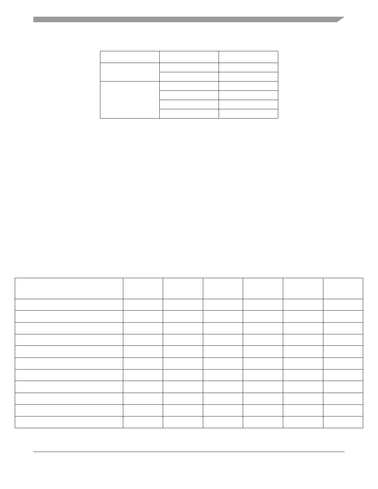
Table 1-6. Port Availability by Package Option
Port 20 TSSOP 32 LQFP
48 LQFP
48 QFN
64 LQFP 100 LQFP KGD (Die)
Port AD/ADC Channels 6 8 12 16 16 16
Port A pins 000088
Port B pins 000088
Port C pins 000088
Port D pins 000088
Port E pins 222222
Port J 004888
Port M 022444
Port P 046888
Port S 468888
Port T 246888
Table 1-5. Assigned Part ID Numbers
Device Mask Set Number Part ID

 Loading...


