Electrical Characteristics
MC9S12G Family Reference Manual Rev.1.27
NXP Semiconductors 1229
In Table A-51 the timing characteristics for master mode are listed.
A.15.2 Slave Mode
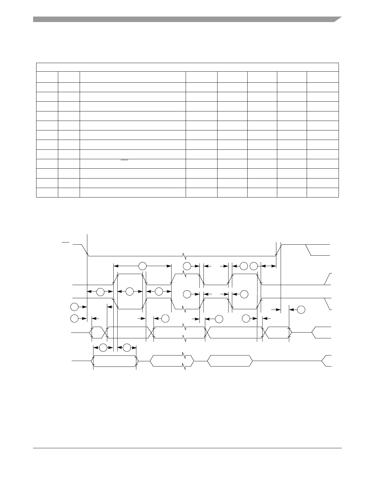
In Figure A-9 the timing diagram for slave mode with transmission format CPHA = 0 is depicted.
Figure A-9. SPI Slave Timing (CPHA = 0)
Table A-51. SPI Master Mode Timing Characteristics
Conditions are 4.5 V < V
DD35
< 5.5 V junction temperature from –40C to T
Jmax
.
Num C Characteristic Symbol Min Typ Max Unit
1 D SCK Frequency
f
sck
1/2048 — 12
f
bus
1 D SCK Period
t
sck
2 — 2048
t
bus
2 D Enable Lead Time
t
L
—1/2—
t
sck
3 D Enable Trail Time
t
T
—1/2—
t
sck
4 D Clock (SCK) High or Low Time
t
wsck
—1/2—
t
sck
5 D Data Setup Time (Inputs)
t
su
8——ns
6 D Data Hold Time (Inputs)
t
hi
8——ns
9 D Data Valid after SCK Edge
t
vsck
——15ns
10 D Data Valid after SS fall (CPHA=0)
t
vss
——15ns
11 D Data Hold Time (Outputs)
t
ho
0——ns
12 D Rise and Fall Time Inputs
t
rfi
—— 9 ns
13 D Rise and Fall Time Outputs
t
rfo
—— 9 ns
SCK
(Input)
SCK
(Input)
MOSI
(Input)
MISO
(Output)
SS
(Input)
1
9
5 6
MSB IN
Bit MSB-1 . . . 1
LSB IN
Slave MSB
Slave LSB OUT
Bit MSB-1. . . 1
11
4
4
2
7
(CPOL = 0)
(CPOL = 1)
3
13
NOTE: Not defined
12
12
11
See
13
Note
8
10
See
Note

 Loading...


