EasyManuals Logo

NXP Semiconductors MC9S12G User Manual

NXP Semiconductors MC9S12G
1277 pages
To Next Page IconTo Next Page
To Previous Page IconTo Previous Page
Page #866 background imageLoading...
Page #866 background image
48 KByte Flash Module (S12FTMRG48K1V1)
MC9S12G Family Reference Manual Rev.1.27
868 NXP Semiconductors
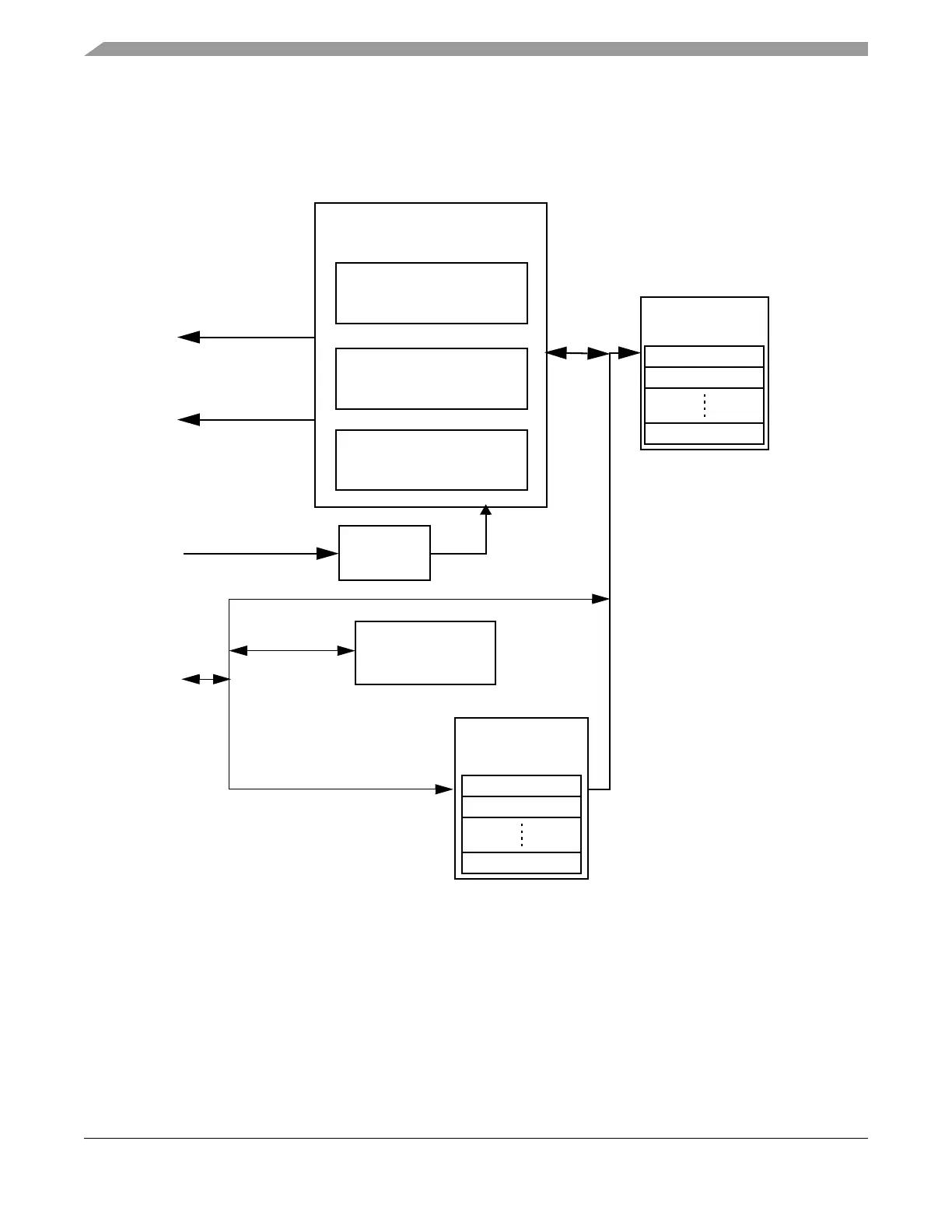
26.1.3 Block Diagram
The block diagram of the Flash module is shown in Figure 26-1.
Figure 26-1. FTMRG48K1 Block Diagram
26.2 External Signal Description
The Flash module contains no signals that connect off-chip.
Bus
Clock
Divider
Clock
Command
Interrupt
Request
FCLK
Protection
Security
Registers
Flash
Interface
16bit
internal
bus
sector 0
sector 1
sector 95
12Kx39
P-Flash
Error
Interrupt
Request
CPU
768x22
sector 0
sector 1
sector 383
EEPROM
Memory Controller

Table of Contents

Questions and Answers:

Question and Answer IconNeed help?

Do you have a question about the NXP Semiconductors MC9S12G and is the answer not in the manual?

NXP Semiconductors MC9S12G Specifications

General IconGeneral
BrandNXP Semiconductors
ModelMC9S12G
CategoryMicrocontrollers
LanguageEnglish

Related product manuals