Electrical Characteristics
MC9S12G Family Reference Manual Rev.1.27
NXP Semiconductors 1197
This constraint exists since the sample buffer amplifier can not drive beyond the power supply levels that
it ties to. If the input level goes outside of this range it will effectively be clipped.
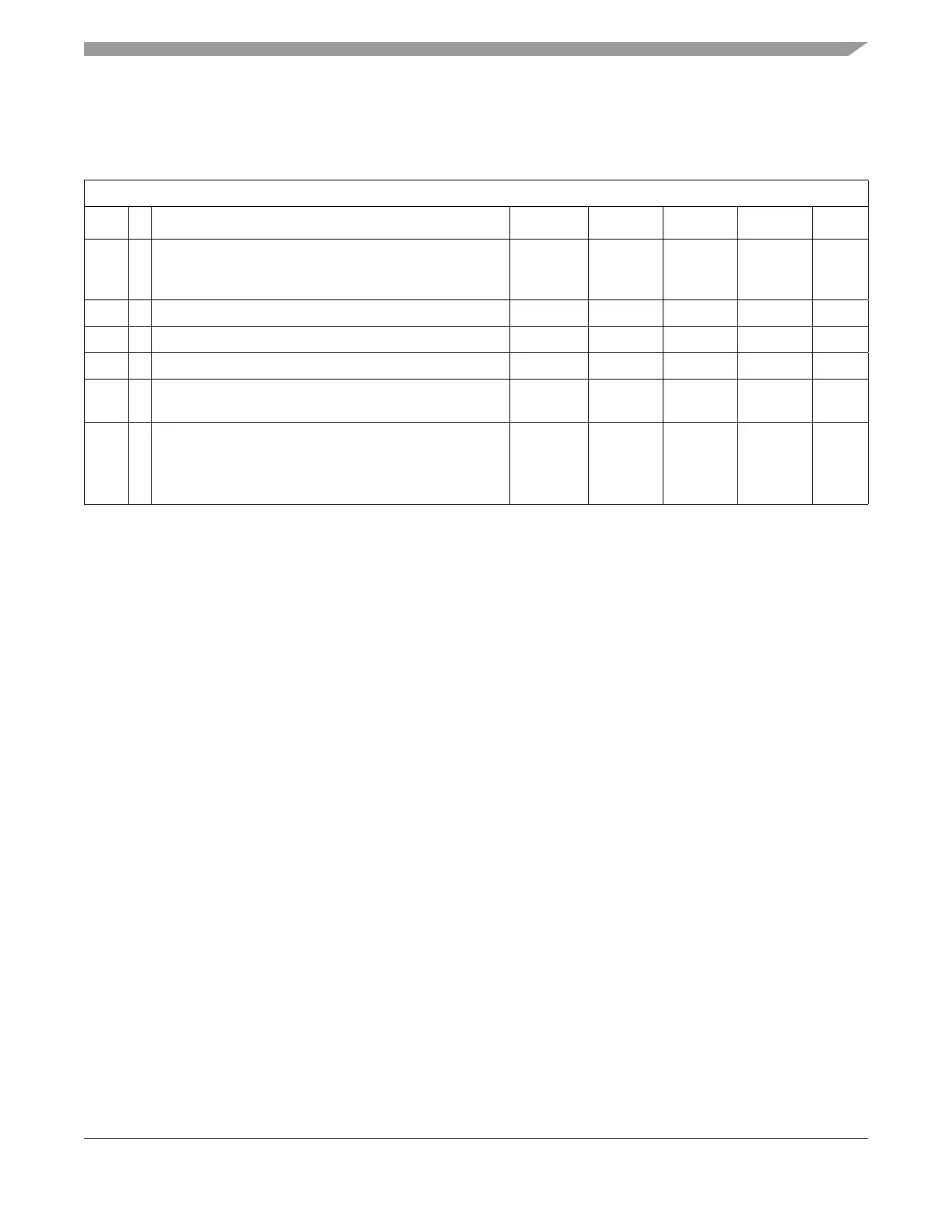
Table A-19. ADC Operating Characteristics
A.4.2 Factors Influencing Accuracy
Source resistance, source capacitance and current injection have an influence on the accuracy of the ADC.
A further factor is that port AD pins that are configured as output drivers switching.
A.4.2.1 Differential Reference Voltage
The accuracy is reduced if the differential reference voltage is less than 3.13V when using the ATD in the
3.3V range or if the differential reference voltage is less than 4.5V when using the ATD in the 5V range.
A.4.2.2 Port AD Output Drivers Switching
Port AD output drivers switching can adversely affect the ADC accuracy whilst converting the analog
voltage on other port AD pins because the output drivers are supplied from the VDDA/VSSA ADC supply
pins. Although internal design measures are implemented to minimize the affect of output driver noise, it
is recommended to configure port AD pins as outputs only for low frequency, low load outputs. The impact
on ADC accuracy is load dependent and not specified. The values specified are valid under condition that
no port AD output drivers switch during conversion.
A.4.2.3 Source Resistance
Due to the input pin leakage current as specified in conjunction with the source resistance there will be a
voltage drop from the signal source to the ADC input. The maximum source resistance R
S
specifies results
Supply voltage 3.13 V < V
DDA
< 5.5 V, -40
o
C < T
J
< T
Jmax
1
1
see Table A-4
Num C Rating Symbol Min Typ Max Unit
1 D Reference potential
Low
High
V
RL
V
RH
V
SSA
V
DDA
/2
—
—
V
DDA
/2
V
DDA
V
V
2 D Voltage difference V
DDX
to V
DDA
VDDX
–2.35 0 0.1 V
3 D Voltage difference V
SSX
to V
SSA
VSSX
–0.1 0 0.1 V
4 C Differential reference voltage V
RH
-V
RL
3.13 5.0 5.5 V
5 C ADC Clock Frequency (derived from bus clock via the
prescaler bus) f
ATDCLk
0.25 8.0 MHz
8D
ADC Conversion Period
2
12 bit resolution:
10 bit resolution:
8 bit resolution:
2
The minimum time assumes a sample time of 4 ADC clock cycles. The maximum time assumes a sample time of 24 ADC
clock cycles and the discharge feature (SMP_DIS) enabled, which adds 2 ADC clock cycles.
N
CONV12
N
CONV10
N
CONV8
20
19
17
42
41
39
ADC
clock
Cycles

 Loading...


