S12G Memory Map Controller (S12GMMCV1)
MC9S12G Family Reference Manual Rev.1.27
NXP Semiconductors 261
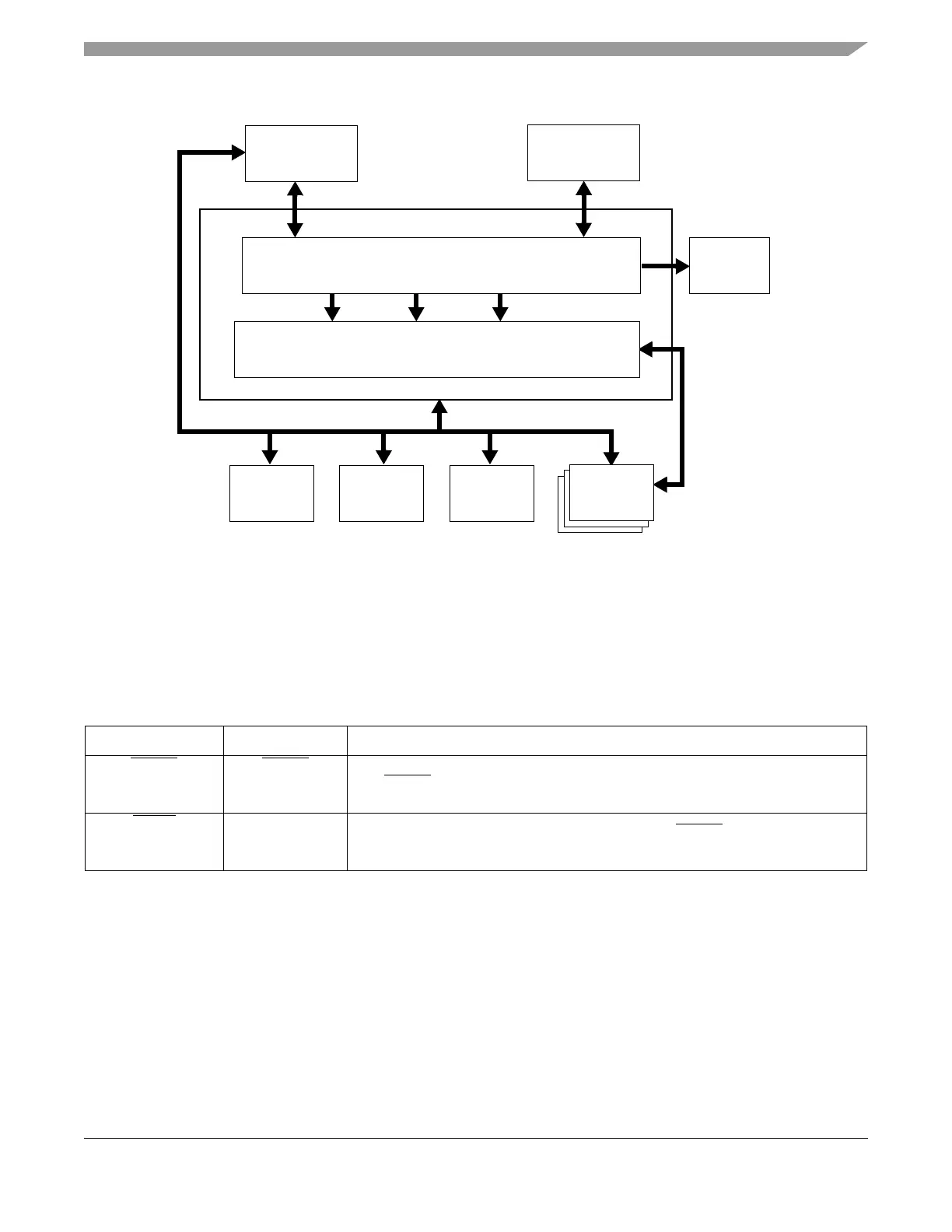
Figure 5-1. S12GMMC Block Diagram
5.2 External Signal Description
The S12GMMC uses two external pins to determine the devices operating mode: RESET and MODC
(Figure 5-3) See Device User Guide (DUG) for the mapping of these signals to device pins.
5.3 Memory Map and Registers
5.3.1 Module Memory Map
A summary of the registers associated with the S12GMMC block is shown in Figure 5-2. Detailed
descriptions of the registers and bits are given in the subsections that follow.
Table 5-3. External System Pins Associated With S12GMMC
Pin Name Pin Functions Description
RESET
(See Section
Device Overview)
RESET
The RESET pin is used the select the MCU’s operating mode.
MODC
(See Section
Device Overview)
MODC
The MODC pin is captured at the rising edge of the RESET
pin. The captured
value determines the MCU’s operating mode.
CPU
BDM
Target Bus Controller
DBG
MMC
Address Decoder & Priority
Peripherals
FlashEEPROM RAM

 Loading...


