Reference Voltage Attenuator (RVAV1)
MC9S12G Family Reference Manual Rev.1.27
NXP Semiconductors 257
4.6 Memory Map and Register Definition
4.6.1 Register Map
Table 4-1 shows the RVA register map.
Table 4-1. RVA Register Map
4.6.2 Register Descriptions
4.6.2.1 RVA Control Register (RVACTL)
Global Address
Register Name
Bit 7654321Bit 0
0x0276
RVACTL
R0000000
RVAON
W
= Unimplemented or Reserved
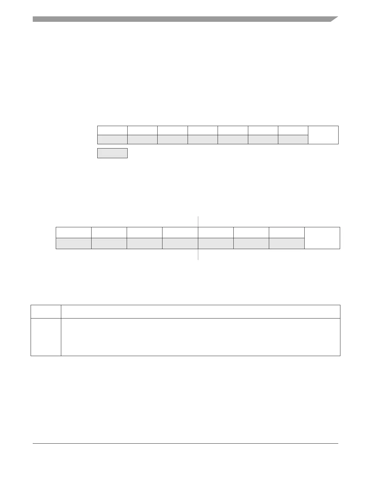
Address 0x0276 Access: User read/write
1
1
Read: Anytime
Write: Anytime
76543210
R0000000
RVAON
W
Reset00000000
Figure 4-2. RVA Control Register (RVACTL)
Table 4-2. RVACTL Register Field Descriptions
Field Description
0
RVAON
RVA On —
This bit turns on the reference voltage attenuation.
0 RVA in bypass mode
1 RVA in attenuation mode

 Loading...


