96 KByte Flash Module (S12FTMRG96K1V1)
MC9S12G Family Reference Manual Rev.1.27
NXP Semiconductors 973
28.3 Memory Map and Registers
This section describes the memory map and registers for the Flash module. Read data from unimplemented
memory space in the Flash module is undefined. Write access to unimplemented or reserved memory space
in the Flash module will be ignored by the Flash module.
CAUTION
Writing to the Flash registers while a Flash command is executing (that is
indicated when the value of flag CCIF reads as ’0’) is not allowed. If such
action is attempted the write operation will not change the register value.
Writing to the Flash registers is allowed when the Flash is not busy
executing commands (CCIF = 1) and during initialization right after reset,
despite the value of flag CCIF in that case (refer to Section 28.6 for a
complete description of the reset sequence).
.
28.3.1 Module Memory Map
The S12 architecture places the P-Flash memory between global addresses 0x2_8000 and 0x3_FFFF as
shown in Table 28-3.The P-Flash memory map is shown in Figure 28-2.
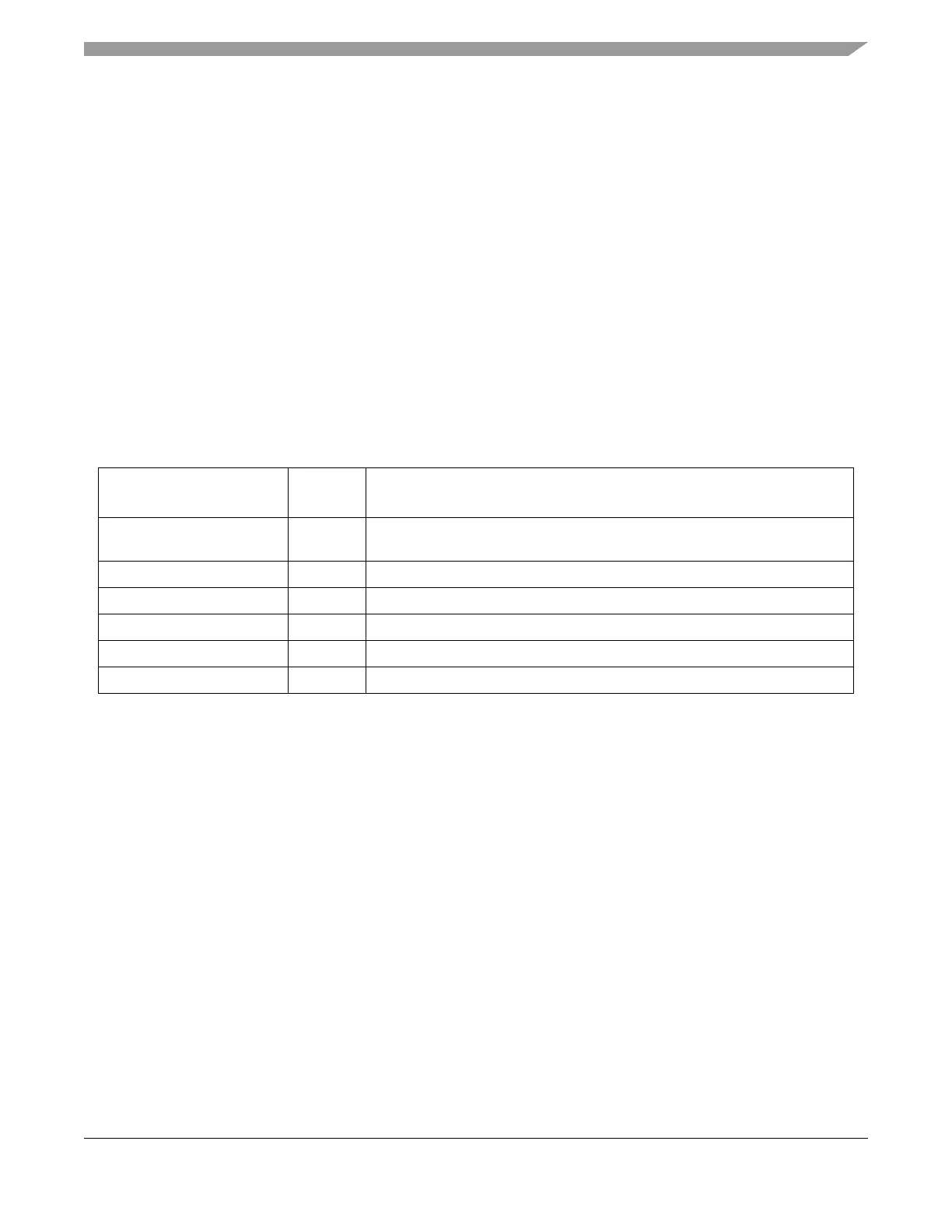
Table 28-2. FTMRG Memory Map
Global Address (in Bytes) Size
(Bytes)
Description
0x0_0000 - 0x0_03FF
1,024
Register Space
0x0_0400 – 0x0_0FFF 3,072 EEPROM Memory
0x0_1000 – 0x0_13FF 1,024 FTMRG reserved area
0x0_4000 – 0x0_7FFF 16,284 NVMRES
1
=1 : NVM Resource area (see Figure 28-3)
1
See NVMRES description in Section 28.4.3
0x2_0000 – 0x2_7FFF 32,767 FTMRG reserved area
0x2_8000 – 0x3_FFFF 98,304 P-Flash Memory

 Loading...


