Serial Peripheral Interface (S12SPIV5)
MC9S12G Family Reference Manual Rev.1.27
NXP Semiconductors 693
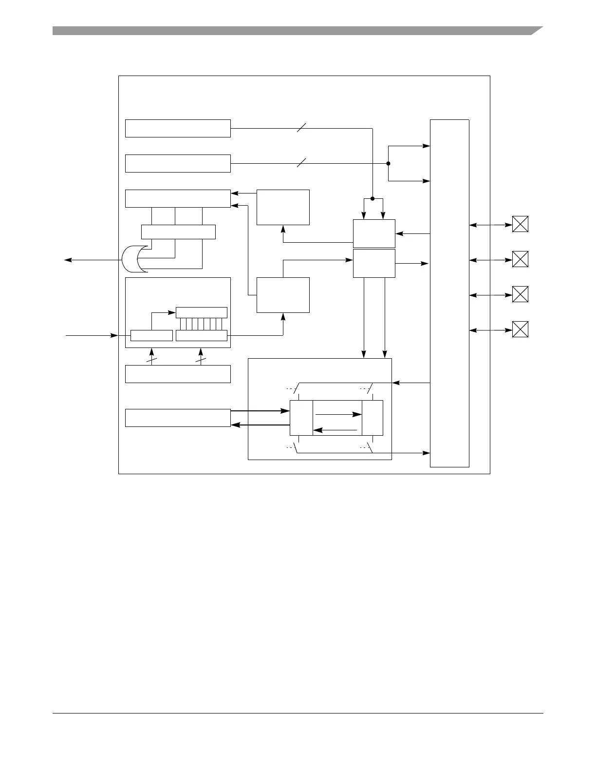
Figure 21-1. SPI Block Diagram
21.2 External Signal Description
This section lists the name and description of all ports including inputs and outputs that do, or may, connect
off chip. The SPI module has a total of four external pins.
21.2.1 MOSI — Master Out/Slave In Pin
This pin is used to transmit data out of the SPI module when it is configured as a master and receive data
when it is configured as slave.
SPI Control Register 1
SPI Control Register 2
SPI Baud Rate Register
SPI Status Register
SPI Data Register
Shifter
Port
Control
Logic
MOSI
SCK
Interrupt Control
SPI
MSB
LSB
LSBFE=1 LSBFE=0
LSBFE=0 LSBFE=1
Data In
LSBFE=1
LSBFE=0
Data Out
Baud Rate Generator
Prescaler
Bus Clock
Counter
Clock Select
SPPR
3
3
SPR
Baud Rate
Phase +
Polarity
Control
Master
Slave
SCK In
SCK Out
Master Baud Rate
Slave Baud Rate
Phase +
Polarity
Control
Control
Control
CPOL
CPHA
2
BIDIROE
SPC0
2
Shift Sample
ClockClock
MODF
SPIF
SPTEF
SPI
Request
Interrupt
SS

 Loading...


