Digital Analog Converter (DAC_8B5V)
MC9S12G Family Reference Manual Rev.1.27
NXP Semiconductors 563
17.4.2 Register Descriptions
This section consists of register descriptions in address order. Each description includes a standard register
diagram with an associated figure number. Details of register bit and field function follow the register
diagrams, in bit order.
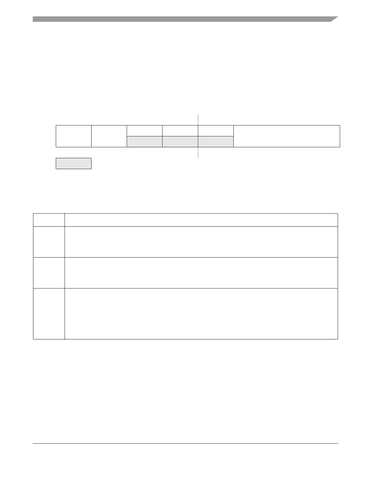
17.4.2.1 Control Register (DACCTL)
)
Module Base + 0x0000 Access: User read/write
1
1
Read: Anytime
Write: Anytime
76543210
R
FVR DRIVE
0 00
DACM[2:0]
W
Reset10000000
= Unimplemented
Figure 17-3. Control Register (DACCTL)
Table 17-3. DACCTL Field Description
Field Description
7
FVR
Full Voltage Range — This bit defines the voltage range of the DAC.
0 DAC resistor network operates with the reduced voltage range
1 DAC resistor network operates with the full voltage range
Note: For more details see Section 17.5.7, “Analog output voltage calculation”.
6
DRIVE
Drive Select — This bit selects the output drive capability of the operational amplifier, see electrical Spec. for more
details.
0 Low output drive for high resistive loads
1 High output drive for low resistive loads
2:0
DACM[2:0]
Mode Select — These bits define the mode of the DAC. A write access with an unsupported mode will be ignored.
000 Off
001 Operational Amplifier
100 Unbuffered DAC
101 Unbuffered DAC with Operational Amplifier
111 Buffered DAC
other Reserved

 Loading...


