Scalable Controller Area Network (S12MSCANV3)
MC9S12G Family Reference Manual Rev.1.27
574 NXP Semiconductors
18.3.2 Register Descriptions
This section describes in detail all the registers and register bits in the MSCAN module. Each description
includes a standard register diagram with an associated figure number. Details of register bit and field
function follow the register diagrams, in bit order. All bits of all registers in this module are completely
synchronous to internal clocks during a register read.
18.3.2.1 MSCAN Control Register 0 (CANCTL0)
The CANCTL0 register provides various control bits of the MSCAN module as described below.
0x000E
CANRXERR
R RXERR7 RXERR6 RXERR5 RXERR4 RXERR3 RXERR2 RXERR1 RXERR0
W
0x000F
CANTXERR
R TXERR7 TXERR6 TXERR5 TXERR4 TXERR3 TXERR2 TXERR1 TXERR0
W
0x0010–0x0013
CANIDAR0–3
R
AC7AC6AC5AC4AC3AC2AC1AC0
W
0x0014–0x0017
CANIDMRx
R
AM7 AM6 AM5 AM4 AM3 AM2 AM1 AM0
W
0x0018–0x001B
CANIDAR4–7
R
AC7AC6AC5AC4AC3AC2AC1AC0
W
0x001C–0x001F
CANIDMR4–7
R
AM7 AM6 AM5 AM4 AM3 AM2 AM1 AM0
W
0x0020–0x002F
CANRXFG
R
See Section 18.3.3, “Programmer’s Model of Message Storage”
W
0x0030–0x003F
CANTXFG
R
See Section 18.3.3, “Programmer’s Model of Message Storage”
W
Register
Name
Bit 7654321Bit 0
= Unimplemented or Reserved
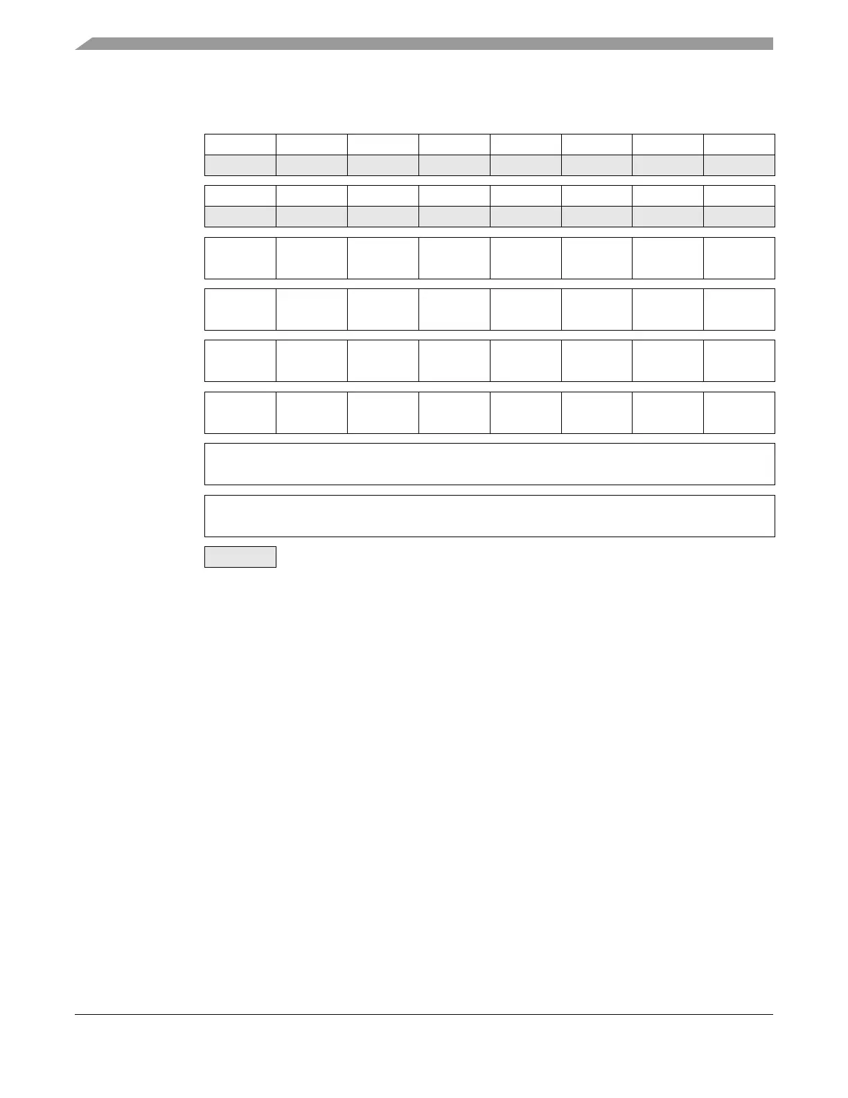
Figure 18-3. MSCAN Register Summary (continued)

 Loading...


