Port Integration Module (S12GPIMV1)
MC9S12G Family Reference Manual Rev.1.27
180 NXP Semiconductors
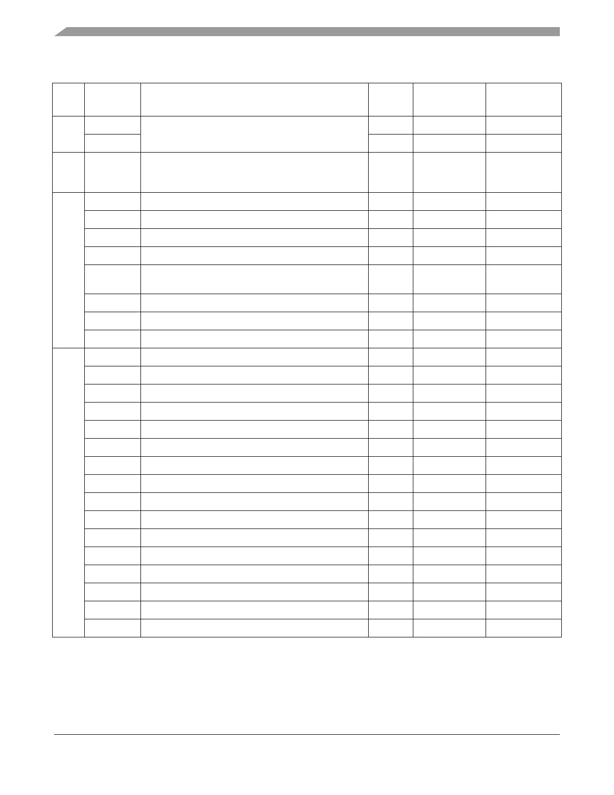
0x0260 Reserved for ACMP available in group G2 and G3 R(/W) 0x00 (ACMP)
0x0261 R(/W) 0x00 (ACMP)
0x0262
:
0x0266
Reserved R 0x00
J 0x0268 PTJ—Port J Data Register R/W 0x00 2.4.3.42/2-226
0x0269 PTIJ—Port J Input Register R
3
2.4.3.43/2-227
0x026A DDRJ—Port J Data Direction Register R/W 0x00 2.4.3.44/2-227
0x026B Reserved R 0x00
0x026C PERJ—Port J Pull Device Enable Register R/W 0xFF (G1,G2)
0x0F (G3)
2.4.3.45/2-228
0x026D PPSJ—Port J Polarity Select Register R/W 0x00 2.4.3.46/2-229
0x026E PIEJ—Port J Interrupt Enable Register R/W 0x00 2.4.3.47/2-229
0x026F PIFJ—Port J Interrupt Flag Register R/W 0x00 2.4.3.48/2-230
AD 0x0270 PT0AD—Port AD Data Register R/W 0x00 2.4.3.49/2-231
0x0271 PT1AD—Port AD Data Register R/W 0x00 2.4.3.50/2-231
0x0272 PTI0AD—Port AD Input Register R
3
2.4.3.51/2-232
0x0273 PTI1AD—Port AD Input Register R
3
2.4.3.54/2-233
0x0274 DDR0AD—Port AD Data Direction Register R/W 0x00 2.4.3.53/2-233
0x0275 DDR1AD—Port AD Data Direction Register R/W 0x00 2.4.3.54/2-233
0x0276 Reserved for RVACTL on G(A)240 and G(A)192 only R(/W) 0x00 (RVA)
0x0277 PRR1—Pin Routing Register 1
6
R/W 0x00 2.4.3.56/2-234
0x0278 PER0AD—Port AD Pull Device Enable Register R/W 0x00 2.4.3.57/2-235
0x0279 PER1AD—Port AD Pull Device Enable Register R/W 0x00 2.4.3.58/2-236
0x027A PPS0AD—Port AD Polarity Select Register R/W 0x00 2.4.3.59/2-236
0x027B PPS1AD—Port AD Polarity Select Register R/W 0x00 2.4.3.60/2-237
0x027C PIE0AD—Port AD Interrupt Enable Register R/W 0x00 2.4.3.61/2-238
0x027D PIE1AD—Port AD Interrupt Enable Register R/W 0x00 2.4.3.62/2-238
0x027E PIF0AD—Port AD Interrupt Flag Register R/W 0x00 2.4.3.63/2-239
0x027F PIF1AD—Port AD Interrupt Flag Register R/W 0x00 2.4.3.64/2-240
1
Available in group G1 only. In any other case this address is reserved.
2
Refer to device memory map to determine related module.
3
Read always returns logic level on pins.
4
Routing takes only effect if the PKGCR is set to 20 TSSOP.
Table 2-18. Block Memory Map (0x0000-0x027F) (continued)
Port
Global
Address
Register Access Reset Value Section/Page

 Loading...


