Port Integration Module (S12GPIMV1)
MC9S12G Family Reference Manual Rev.1.27
NXP Semiconductors 229
2.4.3.46 Port J Polarity Select Register (PPSJ)
2.4.3.47 Port J Interrupt Enable Register (PIEJ)
Read: Anytime
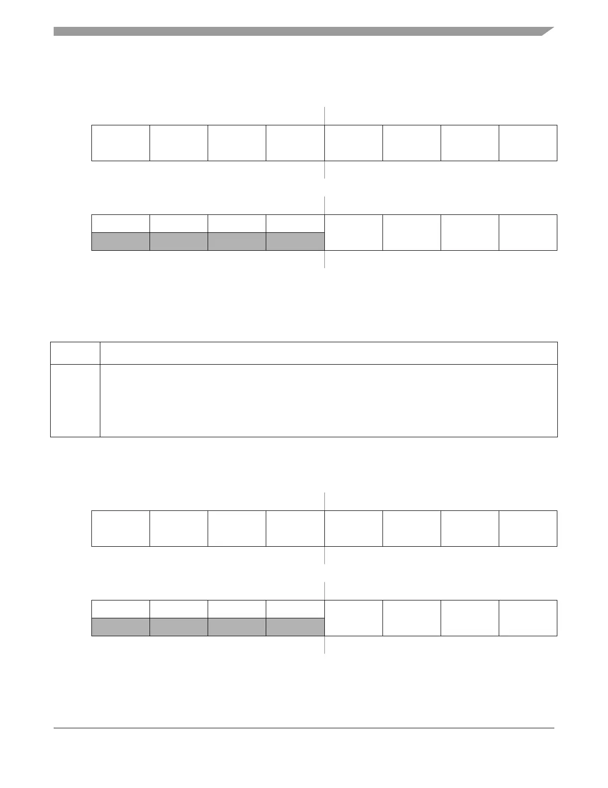
Address 0x026D (G1, G2) Access: User read/write
1
1
Read: Anytime
Write: Anytime
76543210
R
PPSJ7 PPSJ6 PPSJ5 PPSJ4 PPSJ3 PPSJ2 PPSJ1 PPSJ0
W
Reset00000000
Address 0x026D (G3) Access: User read/write
1
76543210
R0000
PPSJ3 PPSJ2 PPSJ1 PPSJ0
W
Reset00000000
Figure 2-46. Port J Polarity Select Register (PPSJ)
Table 2-72. PPSJ Register Field Descriptions
Field Description
7-0
PPSJ
Port J pull device select—Configure pull device and pin interrupt edge polarity on input pin
This bit selects a pullup or a pulldown device if enabled on the associated port input pin.
This bit also selects the polarity of the active pin interrupt edge.
1 Pulldown device selected; rising edge selected
0 Pullup device selected; falling edge selected
Address 0x026E (G1, G2) Access: User read/write
1
76543210
R
PIEJ7 PIEJ6 PIEJ5 PIEJ4 PIEJ3 PIEJ2 PIEJ1 PIEJ0
W
Reset00000000
Address 0x026E (G3) Access: User read/write
1
76543210
R0000
PIEJ3 PIEJ2 PIEJ1 PIEJ0
W
Reset00000000
Figure 2-47. Port J Interrupt Enable Register (PIEJ)

 Loading...


