Port Integration Module (S12GPIMV1)
MC9S12G Family Reference Manual Rev.1.27
234 NXP Semiconductors
2.4.3.55 Reserved Register
NOTE
Address 0x0276 is reserved for RVA on G(A)240 and G(A)192 only. Refer
to RVA section “RVA Control Register (RVACTL)”.
2.4.3.56 Pin Routing Register 1 (PRR1)
NOTE
Routing takes only effect if PKGCR is set to select the 100 LQFP package.
Table 2-80. DDR1AD Register Field Descriptions
Field Description
7-0
DDR1AD
Port AD data direction—
This bit determines whether the associated pin is an input or output.
1 Associated pin configured as output
0 Associated pin configured as input
Address 0x0277 (G(A)240 and G(A)192 only) Access: User read/write
1
1
Read: Anytime
Write: Anytime
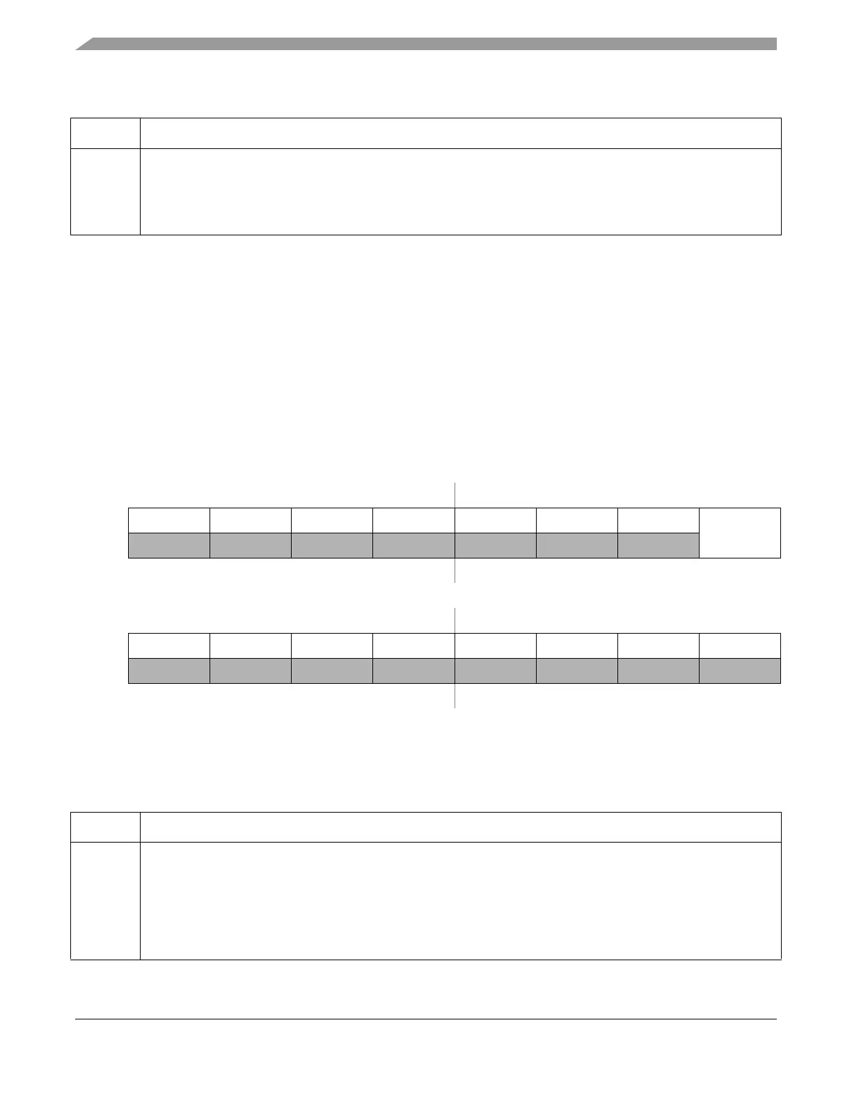
76543210
R0000000
PRR1AN
W
Reset00000000
Address 0x0277 (non G(A)240 and G(A)192) Access: User read/write
76543210
R00000000
W
Reset00000000
Figure 2-55. Pin Routing Register (PRR1)
Table 2-81. PRR1 Register Field Descriptions
Field Description
0
PRR1AN
Pin Routing Register ADC channels — Select alternative routing for AN15/14/13/11/10 pins to port C
This bit programs the routing of the specific ADC channels to alternative external pins in 100 LQFP. See Table 2-82.
The routing affects the analog signals and digital input trigger paths to the ADC. Refer to the related pin descriptions
in Section 2.3.4, “Pins PC7-0” and Section 2.3.12, “Pins AD15-0”.
1 AN inputs on port C
0 AN inputs on port AD

 Loading...


