Port Integration Module (S12GPIMV1)
MC9S12G Family Reference Manual Rev.1.27
NXP Semiconductors 233
2.4.3.53 Port AD Data Direction Register (DDR0AD)
2.4.3.54 Port AD Data Direction Register (DDR1AD)
Table 2-78. PTI1AD Register Field Descriptions
Field Description
7-0
PTI1AD
Port AD input data—
A read always returns the buffered input state of the associated pin. It can be used to detect overload or short circuit
conditions on output pins.
Address 0x0274 (G1, G2) Access: User read/write
1
1
Read: Anytime
Write: Anytime
76543210
R
DDR0AD7 DDR0AD6 DDR0AD5 DDR0AD4 DDR0AD3 DDR0AD2 DDR0AD1 DDR0AD0
W
Reset00000000
Address 0x0274 (G3) Access: User read/write
1
76543210
R0000
DDR0AD3 DDR0AD2 DDR0AD1 DDR0AD0
W
Reset00000000
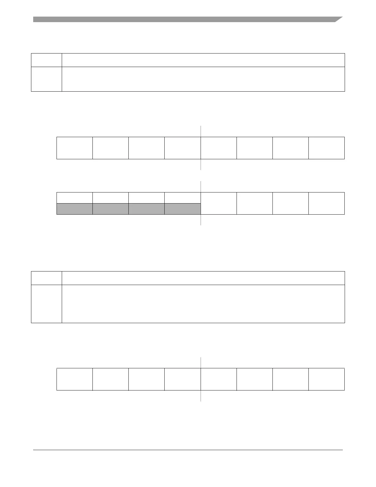
Figure 2-53. Port AD Data Direction Register (DDR0AD)
Table 2-79. DDR0AD Register Field Descriptions
Field Description
7-0
DDR0AD
Port AD data direction—
This bit determines whether the associated pin is an input or output.
1 Associated pin configured as output
0 Associated pin configured as input
Address 0x0275 Access: User read/write
1
1
Read: Anytime
Write: Anytime
76543210
R
DDR1AD7 DDR1AD6 DDR1AD5 DDR1AD4 DDR1AD3 DDR1AD2 DDR1AD1 DDR1AD0
W
Reset00000000
Figure 2-54. Port AD Data Direction Register (DDR1AD)

 Loading...


