Electrical Characteristics
MC9S12G Family Reference Manual Rev.1.27
1212 NXP Semiconductors
Each command timing is given by:
The timing parameters are captured exclusively during command execution (CCIF=0), excluding any time
spent on the command write sequence to load and start the command. The formula above and the number
of cycles in the following tables apply for the cases where the commands executed successfully in a new
device, reflected in the minimum and typical timing parameters; however, due to aging, some of the
commands will adjust their execution according to different margin settings and may eventually take
longer to run than what the formula may return. The Max and Lfmax timing columns in the tables below
already reflect this adjustment where applicable.
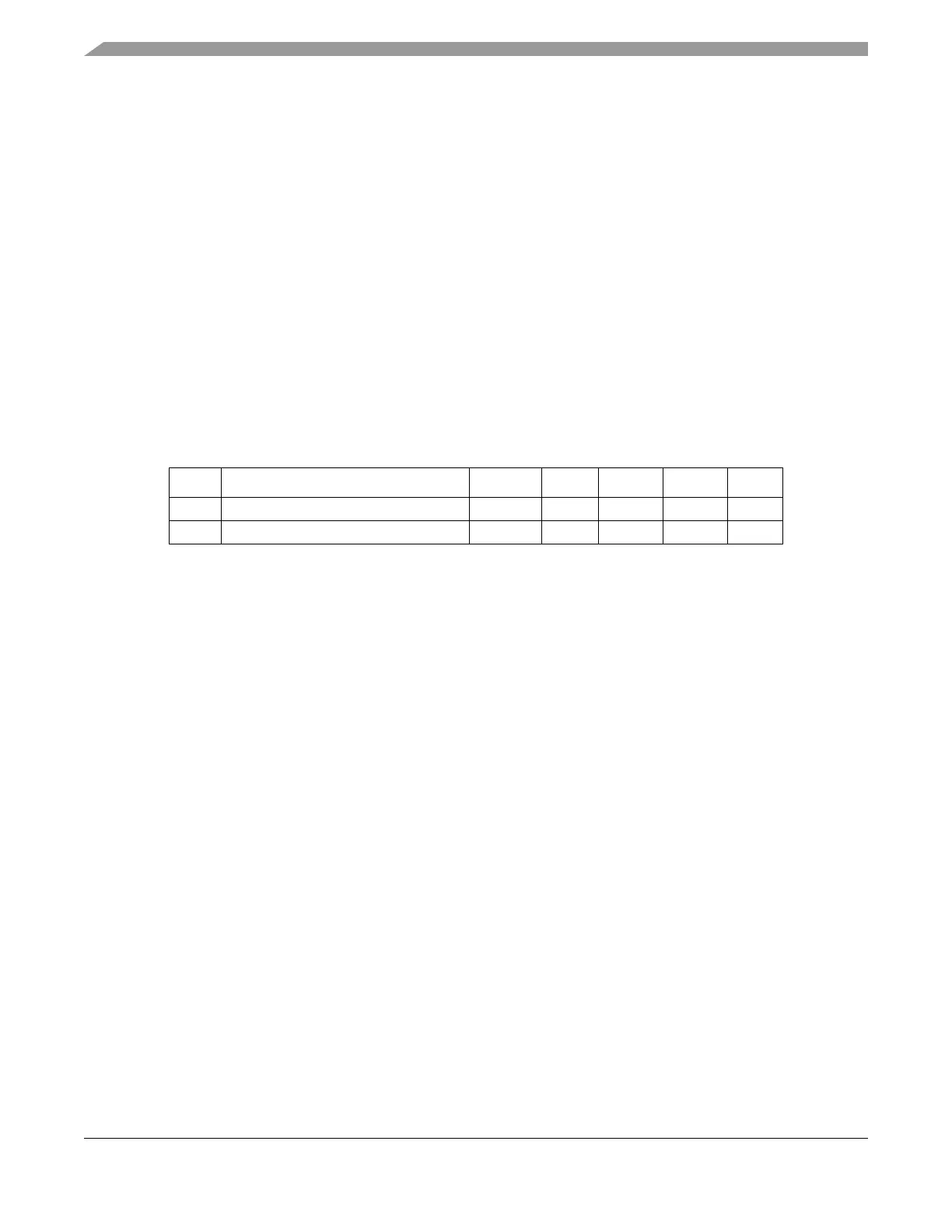
A summary of key timing parameters can be found from Table A-34 to Table A-38.
Table A-34. NVM Clock Timing Characteristics
Num Rating Symbol Min Typ Max Unit
1 Bus frequency f
NVMBUS
12525MHz
2 Operating frequency f
NVMOP
0.8 1.0 1.05 MHz
t
command
f
NVMOP cycle
1
f
NVMOP
---------------------
f
NVMBUS cycle
1
f
NVMBUS
-------------------------
+
=

 Loading...


