Electrical Characteristics
MC9S12G Family Reference Manual Rev.1.27
NXP Semiconductors 1213
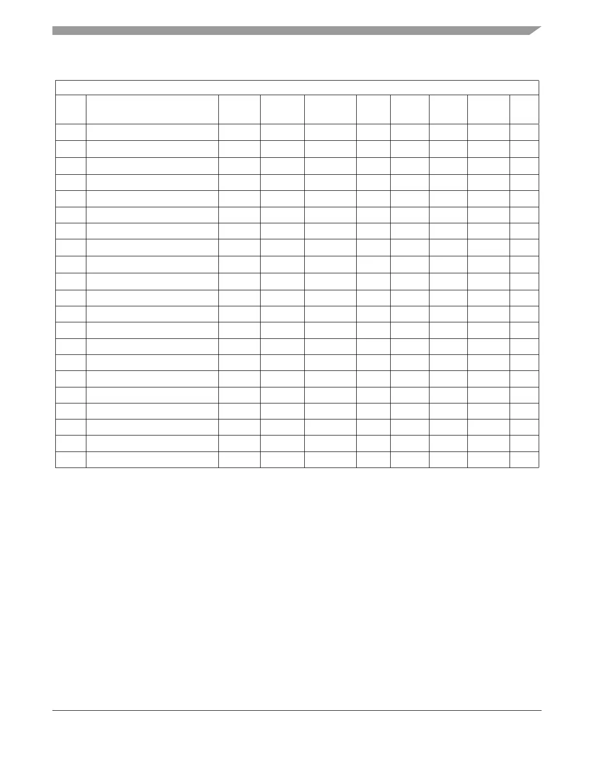
Table A-35. NVM Timing Characteristics)
S12GN16, S12GNA16, S12GN32, S12GNA32
Num Command
f
NVMOP
cycle
f
NVMBUS
cycle
Symbol Min
1
Typ
2
Max
3
Lfmax
4
Unit
1
Erase Verify All Blocks
5,6
09233
t
RD1ALL
0.37 0.37 0.74 18.47 ms
2
Erase Verify Block (Pflash)
5
08737
t
RD1BLK_P
0.35 0.35 0.7 17.47 ms
3
Erase Verify Block (EEPROM)
6
01000
t
RD1BLK_D
0.04 0.04 0.08 2 ms
4 Erase Verify P-Flash Section 0 486
t
RD1SEC
19.44 19.44 38.88 972 ms
5 Read Once 0 445
t
RDONCE
17.8 17.8 17.8 445 s
6 Program P-Flash (4 Word) 164 2935
t
PGM_4
0.27 0.28 0.63 11.95 ms
7 Program Once 164 2888
t
PGMONCE
0.27 0.28 0.28 3.09 ms
8
Erase All Blocks
5,6
100066 9569
t
ERSALL
95.68 100.45 100.83 144.22 ms
9
Erase Flash Block (Pflash)
5
100060 8975
t
ERSBLK_P
95.65 100.42 100.78 143.03 ms
10
Erase Flash Block (EEPROM)
6
100060 1296
t
ERSBLK_D
95.35 100.11 100.16 127.67 ms
11 Erase P-Flash Sector 20015 875
t
ERSPG
19.1 20.05 20.09 26.77 ms
12 Unsecure Flash 100066 9647
t
UNSECU
95.69 100.45 100.84 144.38 ms
13 Verify Backdoor Access Key 0 481
t
VFYKEY
19.24 19.24 19.24 481 s
14 Set User Margin Level 0 404
t
MLOADU
16.16 16.16 16.16 404 s
15 Set Factory Margin Level 0 413
t
MLOADF
16.52 16.52 16.52 413 s
16 Erase Verify EEPROM Section 0 546
t
DRD1SEC
0.02 0.02 0.04 1.09 ms
17 Program EEPROM (1 Word) 68 1565
t
DPGM_1
0.13 0.13 0.32 6.35 ms
18 Program EEPROM (2 Word) 136 2512
t
DPGM_2
0.23 0.24 0.54 10.22 ms
19 Program EEPROM (3 Word) 204 3459
t
DPGM_3
0.33 0.34 0.76 14.09 ms
20 Program EEPROM (4 Word) 272 4406
t
DPGM_4
0.44 0.45 0.98 17.96 ms
21 Erase EEPROM Sector 5015 753
t
DERSPG
4.81 5.05 20.57 37.88 ms
1
Minimum times are based on maximum f
NVMOP
and maximum f
NVMBUS
2
Typical times are based on typical f
NVMOP
and typical f
NVMBUS
3
Maximum times are based on typical f
NVMOP
and typical f
NVMBUS
plus aging
4
Lowest-frequency max times are based on minimum f
NVMOP
and minimum f
NVMBUS
plus aging
5
Affected by Pflash size
6
Affected by EEPROM size

 Loading...


