Electrical Characteristics
MC9S12G Family Reference Manual Rev.1.27
1188 NXP Semiconductors
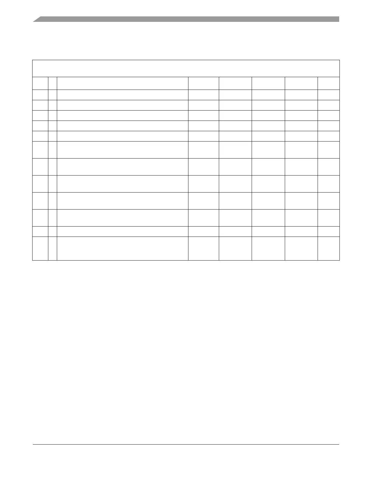
Table A-7. 3.3-V I/O Characteristics (Junction Temperature From +150C To +160C)
Conditions are 3.15 V < V
DD35
< 3.6 V junction temperature from +150C to +160C, unless otherwise noted
I/O Characteristics for all I/O pins except EXTAL, XTAL,TEST and supply pins.
Num C Rating Symbol Min Typ Max Unit
1 M Input high voltage V
IH
0.65*V
DD35
——V
2 T Input high voltage V
IH
——V
DD35
+0.3 V
3 M Input low voltage V
IL
— — 0.35*V
DD35
V
4 T Input low voltage V
IL
V
SS35
– 0.3 — — V
5 C Input hysteresis V
HYS
0.06*V
DD35
—0.3*V
DD35
mV
6 M Input leakage current (pins in high impedance input
mode)
1
V
in
= V
DD35
or V
SS35
1
Maximum leakage current occurs at maximum operating temperature. Current decreases by approximately one-half for each
8°C to 12°C in the temperature range from 50C to 125C.
I
in
-1 — 1 A
7 P Output high voltage (pins in output mode)
I
OH
= –1.75 mA
V
OH
V
DD35
-0.4 — — V
8 C Output low voltage (pins in output mode)
I
OL
= +1.75 mA
V
OL
——
0.4
V
9 M Internal pull up device current
V
IH
min > input voltage > V
IL
max
I
PUL
-1
—
–70
A
10 M Internal pull down device current
V
IH
min > input voltage > V
IL
max
I
PDH
1
—
70
A
11 D Input capacitance C
in
—7—pF
12 T Injection current
2
Single pin limit
Total device limit, sum of all injected currents
2
Refer to Section A.1.4, “Current Injection” for more details
I
ICS
I
ICP
–2.5
–25
—
2.5
25
mA

 Loading...


