Analog-to-Digital Converter (ADC10B12CV2)
MC9S12G Family Reference Manual Rev.1.27
474 NXP Semiconductors
13.3.2.10 ATD Input Enable Register (ATDDIEN)
Read: Anytime
Write: Anytime
13.3.2.11 ATD Compare Higher Than Register (ATDCMPHT)
Writes to this register will abort current conversion sequence.
Read: Anytime
Write: Anytime
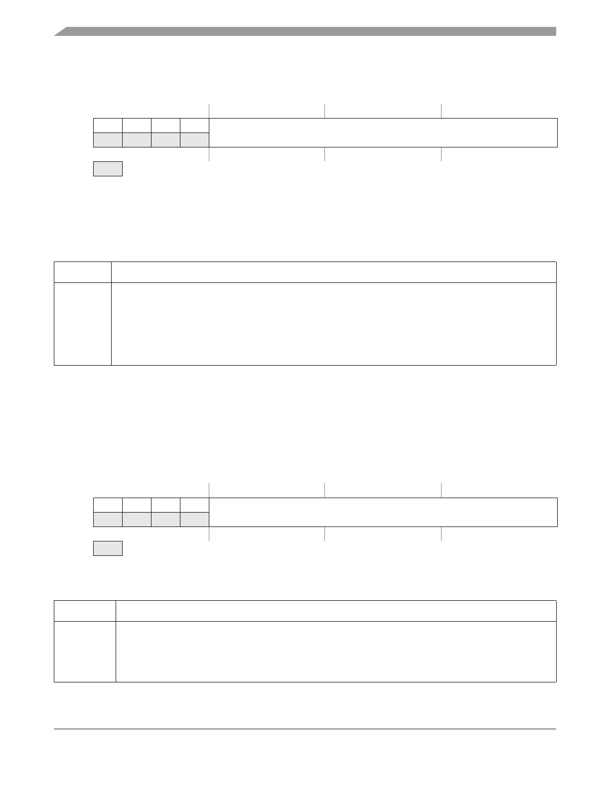
Module Base + 0x000C
15 14 13 12 11 10 9 8 7 6 5 4 3 2 1 0
R 1 1 1 1
IEN[11:0]
W
Reset1111000000000000
= Unimplemented or Reserved
Figure 13-12. ATD Input Enable Register (ATDDIEN)
Table 13-19. ATDDIEN Field Descriptions
Field Description
11–0
IEN[11:0]
ATD Digital Input Enable on channel x (x= 11, 10, 9, 8, 7, 6, 5, 4, 3, 2, 1, 0) — This bit controls the digital input
buffer from the analog input pin (ANx) to the digital data register.
0 Disable digital input buffer to ANx pin
1 Enable digital input buffer on ANx pin.
Note: Setting this bit will enable the corresponding digital input buffer continuously. If this bit is set while
simultaneously using it as an analog port, there is potentially increased power consumption because the
digital input buffer maybe in the linear region.
Module Base + 0x000E
15 14 13 12 11 10 9 8 7 6 5 4 3 2 1 0
R 0 0 0 0
CMPHT[11:0]
W
Reset0000000000000000
= Unimplemented or Reserved
Figure 13-13. ATD Compare Higher Than Register (ATDCMPHT)
Table 13-20. ATDCMPHT Field Descriptions
Field Description
11–0
CMPHT[11:0]
Compare Operation Higher Than Enable for conversion number n (n= 11, 10, 9, 8, 7, 6, 5, 4, 3, 2, 1, 0) of
a Sequence (n conversion number, NOT channel number!) — This bit selects the operator for comparison
of conversion results.
0 If result of conversion n is lower or same than compare value in ATDDRn, this is flagged in ATDSTAT2
1 If result of conversion n is higher than compare value in ATDDRn, this is flagged in ATDSTAT2

 Loading...


